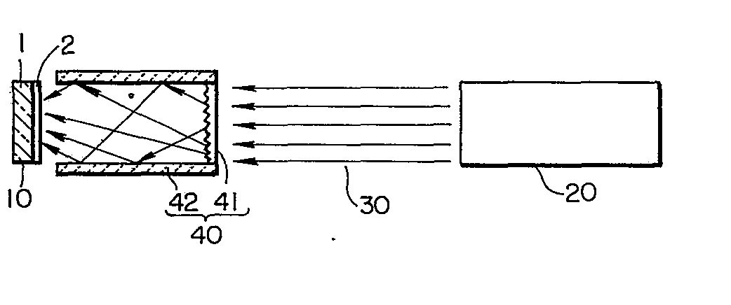
(57) This invention relates to improvements in the SOS technology including the so-called
laser annealing processing. According to this invention, the semiconductor layer (2)
of an SOS structure (1, 2) consists of the three layers of an interface layer made
up of twins, a seed crystalline layer and a re-grown layer far thicker than the preceding
two layers when viewed from the side of an insulating substrate. The re-grown layer
is formed in such a way that the semiconductor layer (2) deposited on the insulating
substrate (1) is irradiated with an electromagnetic wave, for example, a pulsed ruby
laser beam, which is absorbed substantially uniformly by a portion except the interface
layer and the seed crystalline layer. According to this invention, the quality of
the re-grown layer is improved, and the mobility of carriers is enhanced. As a result,
the operating speed of a semiconductor device employing the SOS structure (1, 2) is
raised, and the leakage current is reduced.
|
|
