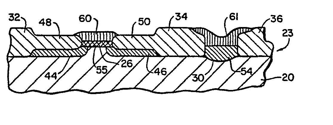
(57) A method of manufacturing devices in a semiconductor body 20 of a first conductivity
type. An oxygen impervious masking medium 22 is placed on the body 20. Portions of
the medium 22 are removed to define field areas 31 and field oxide is formed in the
field areas. The surface of the silicon wafer 23 is thereafter masked to define gate
areas 26 and electrical contact areas 30. The exposed medium is removed and the exposed
body areas doped to form interconnect runs 28 and a source/drain region 29 of a second
conductivity type. An oxide 48, 50 is formed over the doped interconnect runs and
source/drain regions of the wafer. The masking medium covering the contact area 30
is removed and the contact area is doped to a second conductivity type. Finally conductors
60, 61 are positioned to provide the desired electrical connections. In a first alternate
embodiment the masking medium is a sandwich of different material layers 70, 72 and
in a second alternate embodiment the masking medium is a sandwich of three different
layers 80, 82 and 84.
|
|
