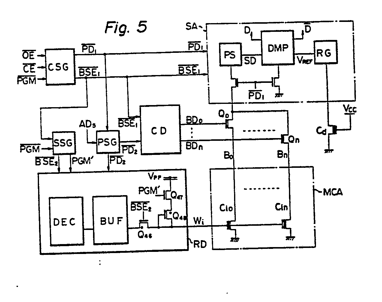
(57) A semiconductor memory device comprises a plurality of memory cell transistors (Cio
-Cin) each of which is disposed at an intersection of a word line (Wi) and a bit line
(Bo - Bn) and each of which has a control gate connected to one of the word lines
and a floating gate which stores electrons. A first power supply input (Vcc) receives
a usual operating voltage, and a second power supply input (Vpp) receives a high voltage
for programming the memory device. The device further comprises a circuit (047, Q48)
which connects the second power supply input to one or more selected word lines (Wi)
when measurement of the threshold potential (Vth) of the memory cell transistors is
to be carried out, the first power supply input voltage being maintained constant,
and the potential of the second power supply input (Vpp) being changed to effect the
measurement of the threshold potential.
|
|
