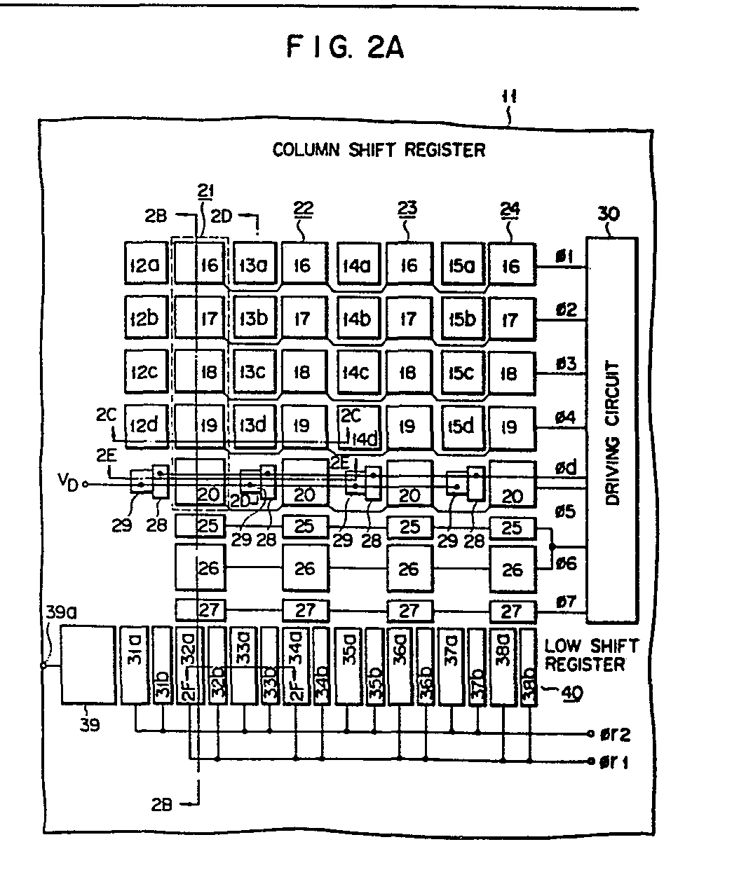
(57) A charge transfer type area image sensor comprises a plurality of photosensitive
picture elements (12a to 12d; 13a to 13d; 14a to 14d; 15a to 15d) arranged on a semiconductor
substrate (11) in a plurality of columns and rows. Columnar groups (21 to 24) of shift
registers including a plurality of charge transfer electrodes (16 to 20) are disposed
adjacent to the respective columnar groups of photosensitive picture elements. Storage
electrodes (25, 26) are provided between the columnar groups (21 to 24) of shift registers
and a row-directed shift register (40) for sending forth output signals to temporarily
store signal charges generated in the photosensitive picture elements. Signal charges
generated in photosensitive picture elements and then transmitted to the corresponding
columnar groups (21 to 24) of shift registers in response to a first selection signal
are temporarily stored under the storage electrodes (25, 26) and then conducted to
the row-directed shift register (40) to be sent forth therefrom as series signal charges.
Excess charges generated and then transmitted to the corresponding columnar groups
of shift registers in response to a second selection signal are discharged to drains
(29) through control electrodes (28) positioned adjacent to the last charge transfer
electrodes of the respective columnar groups (21 to 24) of shift registers, thereby
assuring improvement in the integration density of photosensitive picture elements
and the suppression of blooming.
|
|
