(19)
(11) EP 0 054 355 A3

(12) EUROPEAN PATENT APPLICATION

(88) Date of publication A3:
25.05.1983 Bulletin 1983/21

(43) Date of publication A2:
23.06.1982 Bulletin 1982/25

(21) Application number: 81305348

(22) Date of filing: 11.11.1981
(84) Designated Contracting States:
DE FR GB

(30) Priority: 08.12.1980 JP 17291580
08.12.1980 JP 17291680
08.12.1980 JP 17291780
20.12.1980 JP 18095380
30.07.1981 JP 11978081
30.07.1981 JP 11978181

(71) Applicant: KABUSHIKI KAISHA TOSHIBA
 ()

(72) Inventor:
  • Masuoka, Fujio
     ()


(54) Semiconductor memory device


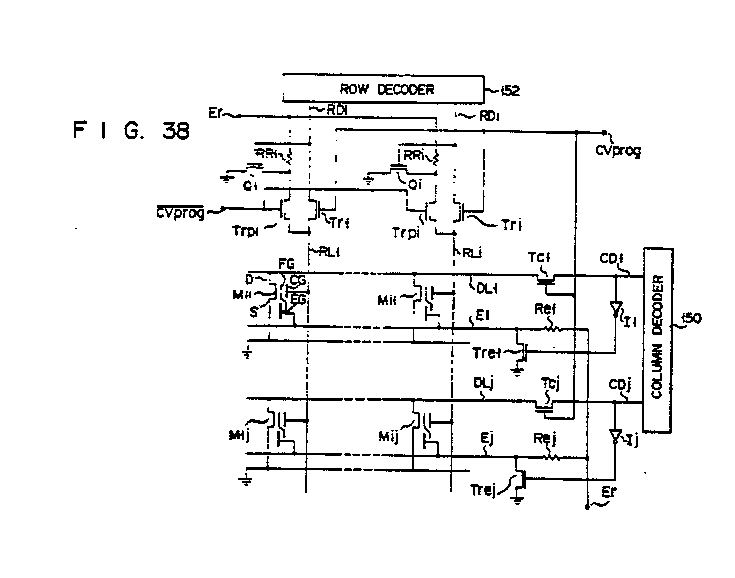
(57) A semiconductor memory device constituted by an MOS transistor which has a control gate (CG) and a floating gate (FG) capable of storing data. An erase gate (EG) is further provided to discharge electrons from the floating gate by field emission. The semiconductor memory device is further provided with a first voltage supply circuit (Er, Trej, Rej, lj, CVprog, Tcj) for supplying a voltage of higher level for erasing the data to the erase gate and a second voltage supply circuit (Tri, Trpi, Oi, CVprog, CVprog) for supplying a voltage of low level to the control gate.


Search report