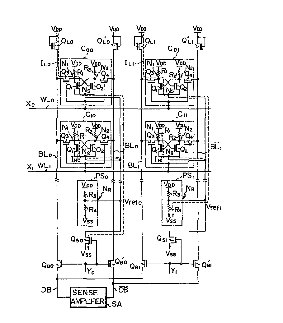
(57) The static memory circuit has rows of memory cells (Coo to C11) defined by word lines WL0, WL, and columns of memory cells defined by pairs of bit lines BL0, BLo; BL,, BL1. Each column has a potential setting circuit PSo, PS1 connected to the memory cells of the column. When a memory cell (e.g. Coo) in a column
is selected the ground side potential of the memory cell is power supply potential
Vss. For a non-selected memory cell (e.g. C01) in a not-selected column the ground side potential is higher than Vss. The ground side potential is at a level Vref1 which is set by potential setting circuit PS1.
|
|
