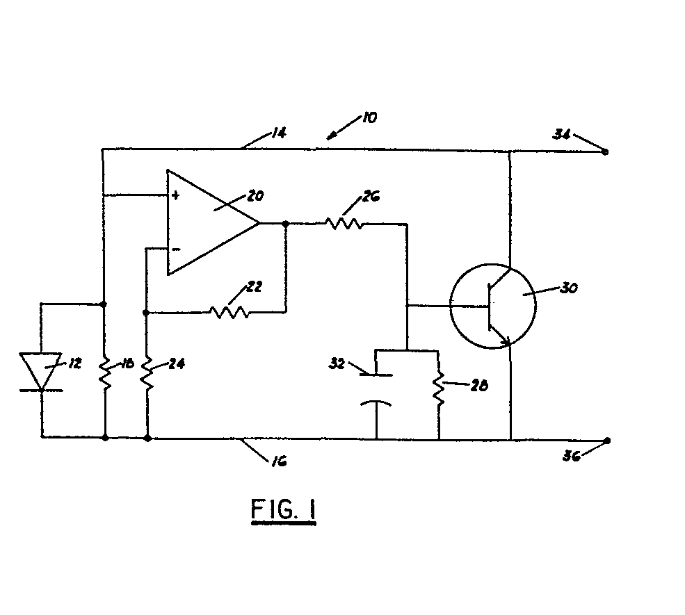
(57) A circuit (10) prevents a photo diode (12) from reaching its saturation output voltage,
thus ensuring the sensitivity of the photo diode to small changes in radiance at high
radiance levels. The circuit (10) utilizes a transistor (30) that is allowed to conduct
after the output voltage of the photo diode (12) has reached a predetermined level,
thus shunt loading the photo diode and preventing it from reaching its saturation
level. A resistor (28) - capacitor (32) time constant circuit is provided to prevent
the transistor (30) from conducting until the output voltage of the photo diode (12)
has reached a predetermined level for a predetermined period of time, thus preventing
premature conduction of the transistor (30) in response to transient or spurious voltages.
|
|
