(57) A semiconductor device having a switching speed of the order of 10-12 seconds is formed in such a way that resonant quantum mechanical transmission of
electric current can occur through a conduction channel (5) between a pair of highly
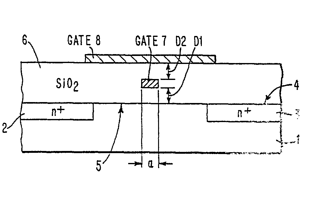
doped electrode regions (2, 3) in a semiconductor substrate (1).
Inner gate electrode means (7; 7A, 78) lies over a central portion of the conduction
channel (5) and is insulated from the surface layer (4) of the substrate. An outer
gate electrode (8) extends completely over the conduction channel (5) and is insulated
from both the conduction channel (5) and the inner gate electrode means (7; 7A, 7B).
The form, size and disposition of the inner gate electrode means and the disposition
of the outer gate electrode are such that by individually biasing the inner gate electrode
means and the outer gate electrode with respect to the substrate a potential well
is formed between two barriers so permitting resonant transmission of electric current
through the conduction channel.
The inner gate electrode means can be either a single electrode having a dimension
of about 100A or at least two closely spaced electrodes. The insulation between the
gates and the channel region can be of the order of 100A thick.
|
|
