| (19) |
 |
|
(11) |
EP 0 110 468 B1 |
| (12) |
EUROPEAN PATENT SPECIFICATION |
| (45) |
Mention of the grant of the patent: |
|
14.05.1986 Bulletin 1986/20 |
| (22) |
Date of filing: 17.11.1983 |
|
| (51) |
International Patent Classification (IPC)4: C30B 23/02 |
|
| (54) |
Method of growing an alloy film by a layer-by-layer process on a substrate, and a
method of making a semiconductor device
Verfahren zum schichtweisen Auftragen eines Legierungsfilmes auf ein Substrat und
Verfahren zum Herstellen eines Halbleiterbauelementes
Méthode pour faire croître un film d'alliage sur un substrat par un procédé couche
par couche, et méthode de fabrication d'un dispositif semi-conducteur
|
| (84) |
Designated Contracting States: |
|
DE FR GB IT NL SE |
| (30) |
Priority: |
26.11.1982 GB 8233778
|
| (43) |
Date of publication of application: |
|
13.06.1984 Bulletin 1984/24 |
| (71) |
Applicants: |
|
- PHILIPS ELECTRONICS UK LIMITED
Croydon CR9 3QR (GB)
GB
- Philips Electronics N.V.
5621 BA Eindhoven (NL)
DE FR IT NL SE
|
|
| (72) |
Inventors: |
|
- Dobson, Peter James
South Croydon
Surrey CR2 6DJ (GB)
- Foxon, Charles Thomas
Redhill
Surrey RH1 5HA (GB)
- Neave, James Hamilton
Redhill
Surrey RH1 5HA (GB)
|
| (74) |
Representative: Boxall, Robin John et al |
|
Philips Electronics UK Limited
Patents and Trade Marks Department
Cross Oak Lane
Redhill, Surrey RH1 5HA
Redhill, Surrey RH1 5HA (GB) |
|
| |
|
| Note: Within nine months from the publication of the mention of the grant of the European
patent, any person may give notice to the European Patent Office of opposition to
the European patent
granted. Notice of opposition shall be filed in a written reasoned statement. It shall
not be deemed to
have been filed until the opposition fee has been paid. (Art. 99(1) European Patent
Convention).
|
[0001] The invention relates to a method of growing an alloy film by a layer-by-layer process
on a substrate, and determining the growth rate of the film by irradiating the growing
alloy film with a beam of electrons and measuring the period of oscillations in the
intensity of the stream of electrons diffracted at the growth surface, of specularly
reflected by the growth surface, or emitted from the growth surface, or of the current
flowing to earth through the substrate, which period is equal to the growth time of
one monolayer of the alloy on the substrate. The invention also relates to a method
of making a semiconductor device, in which method an alloy film is grown on a substrate
by a layer-by-layer process, and the growth rate of the film is determined by irradiating
the growing alloy film with a beam, of electrons and measuring the period of oscillations
in the intensity of the stream of electrons diffracted at the growth surface, or specularly
reflected by the growth surface, or emitted from the growth surface, or of the current
flowing to earth through the substrate, which period is equal to the growth time of
one monolayer of the alloy on the substrate.
[0002] Alloy films may be grown by layer-by-layer processes such as vacuum evaporation or
molecular beam processes. Molecular beam epitaxy processes are widely used in the
manufacture of semiconductor devices, for example, in the fabrication of laser structures,
when it is necessary to deposit III-V alloy films of controlled composition. Hitherto
it has not been possible to determine the composition of an alloy film at it is being
grown. The fluxes of the alloy constituents which are incident on a substrate have
been measured using an ion gauge, or a quartz crystal rate monitor. The compositions
of the alloy films have been measured after the substrates bearing the films have
been removed from the growth systems.
[0003] An article "Oscillations in the surface structure of Sn-doped GaAs during growth
by MBE" by J. J. Harris, B. A. Joyce and P. J. Dobson in Surface Science 103 (1981)
L90L96 states that the presence of predeposited or surface-accumulated Sn during
MBE growth of GaAs modifies the reconstruction of the (001) GaAs surface, as observed
by RHEED, at coverages as low as 0.025 monolayer. It was found that when growth was
initiated on such a surface, oscillations in the intensity modulation of some of the
RHEED streaks occur, with a period equal to the monolayer deposition time of the GaAs.
An article "RED intensity oscillations during MBE of GaAs" by Colin E. C. Wood in
Surface Science 108 (1981) L441-L443 states that while the presence of tin is correctly
identified in the .J. J. Harris et a/ article as the cause of the oscillation, Wood
has found that the pseudo static modulation of (100) oriented c(2 x 8) surface reconstruction
towards "(2 x 3)" and "(1 x 2)" and eventually "(1 x 1)" surfaces to be a universal
effect accompanying heavy n or p type doping, occurring for heavy (-- 2% J
Ga) incident fluxes of Si, Ge, Sn, PbS and PbSe at substrate temperatures at and below
570°C. Wood also observed that in unpublished work he had found that the time dependent
RED streak modulation on arsenic stabilized (2 x 4)(100) tin-accumulated surfaces
was also observed although to a lesser extent, on nominally undoped surfaces.
[0004] An object of the invention is to provide a method of determining the composition
of an alloy film during growth of the film by a layer-by-layer process.
[0005] A method according to the invention of growing an alloy film by a layer-by-layer
process on a substrate, is characterized in that at least one intermediate film consisting
of at least one constituent of the alloy is grown between the substrate and the alloy
film, that the growth rate of the/each intermediate film is determined by irradiating
the growing intermediate film with a beam of electrons and measuring the period of
oscillations in the intensity of the stream of electrons diffracted at the growth
surface, specularly reflected by the growth surface, or emitted from the growth surface,
or of the current flowing to earth through the substrate, and that the atomic ratio
of constituents present in the alloy is calculated from the growth rates of the alloy
film and of the intermediate film(s). The layer-by-layer process may be, for example,
a vacuum evaporation process or a molecular beam epitaxy process.
[0006] Since the growth rate of a film of an alloy AxB,-X is determined by the sum of the
growth rates of the constituents A and B, it follows that the composition of the alloy
can be determined by measuring the growth rates of a buffer layer of the element A
on a substrate and of the alloy AB film grown on this buffer layer, by measuring the
periods of the above-mentioned oscillations to determine the respective growth rates
R
A and R
AB. The atomic fraction x of the element A present in the film of the alloy is given
by

The atomic fraction (1-x) of the element B is given by
[0007] Apparatus used for growing films by molecular beam processes commonly includes an
electron gun and a reflection electron diffraction screen in order to monitor the
cleanness of the substrate surface and the structure of the growth surface. Such apparatus
will not require any additional items such as ion gauges within the growth system
in order to perform a method according to the invention.
[0008] When the alloy is a binary alloy AB, a method according to the invention comprises
the steps of growing a buffer layer of A on the substrate and determining the growth
rate of the buffer layer, growing a film of the alloy AB on the buffer layer by continuing
to deposit A on the growth surface without changing the conditions of the source supplying
A and additionally depositing constituent B of the alloy on the growth surface, determining
the growth rate of the alloy AB film, and calculating the ratio of the growth rate
of the buffer layer to the growth rate of the alloy film which ratio is equal to the
atomic fraction of A present in the alloy AB. Such a binary alloy film may be, for
example, a metal alloy film, such as an Ag-Au film grown by vacuum evaporation on
a silver buffer layer on a (111) NaCl layer present on a mica support, or a silicon-germanium
film grown on a silicon support. When growing a silicon-germanium film, a silicon
buffer layer may be used.
[0009] When the alloy is a ternary III-V alloy ABC in which the elements A and C are group
III elements, a method according to the invention comprises the steps of growing a
buffer layer of the compound AB on the substrate and determining the growth rate of
the buffer layer, growing the film of the alloy ABC by continuing to supply the species
A and B to the growth surface without changing the conditions of the sources supplying
the species A and B and additionally supplying species C to the growth surface, determining
the growth rate of the film of the alloy ABC, cal-- culating the growth rate of the
constituent BC of the alloy ABC by subtracting the growth rate of the buffer layer
AB from the growth rate of the alloy film ABC, and calculating the ratio of the growth
rate of the compound AB to the growth rate of the constituent BC, which ratio is equal
to the atomic ratio A:C in the alloy film ABC. The alloy ABC may be, for example,
Ga
1-
xÄsAl
x, when 1 > x > 0.
[0010] A useful set of oscillations in the intensity of a stream of electrons diffracted
at or specularly reflected by or emitted from the growth surface or flowing to earth
through the substrate is observable at the start of growth, or may be produced, for
example, by momentarily interrupting and then restarting a species flow onto a growth
surface when growing a buffer layer. The intensity of these oscillations falls quite
rapidly, but resumes at a useful level after such an interruption and restart. When
a flow of a further species onto the growth surface is started, a useful set of oscillations
is obtained without it being necessary subsequently to interrupt and restart this
further species flow.
[0011] It is not possible to use a method according to the invention to determine the ratio
of two group V elements present in a III-V alloy containing two group V elements.
There is not a similar limitation in II-VI or IV-VI alloys, since the sticking coefficients
of both the group II and group VI elements, and of the group IV and group VI elements,
in the growth of the respective elements, are interdependent.
[0012] When the alloy is a quaternary III-V alloy ABCD in which elements A and B belong
to different groups of the periodic table; and elements A, C and D belong to group
III, a method according to the invention comprises the steps of growing a buffer layer
of a compound AB on the substrate and determining the growth rate of the buffer layer,
growing a film of an alloy ABC on the buffer layer by continuing to supply species
A and B to the growth surface without changing the conditions of the sources supplying
the species A and B and additionally supplying species C to the growth surface, determining
the growth rate of the film of the alloy ABC, growing a film of the alloy ABCD on
the alloy film'ABC by continuing to supply species A, B and C to the growth surface
without changing the conditions of the sources A, B and C and additionally supplying
species D to the growth surface, and determining the growth rate of the film of the
alloy ABCD, calculating the growth rates of the compounds BC and BD by subtracting
the growth rates of the buffer layer AB and of the film ABC from the growth rates
of the films ABC and ABCD respectively, and calculating the ratios of the growth rate
of the buffer layer to the growth rate of the compound BC to the growth rate of the
compound BD, which ratios are equal to the ratios of the atomic ratios A:C:D in the
alloy film ABCD.
[0013] A method according to the invention of making a semiconductor device, for example,
an injection laser, is characterized in that at least one intermediate film of at
least one constituent of the alloy is grown between the substrate and the alloy film,
that the growth rate of the/each intermediate film is determined by irradiating the
growing intermediate film with a beam of electrons and measuring the period of oscillations
in the intensity of the stream of electrons diffracted at the growth surface specularly
reflected by the growth surface, or emitted from the growth surface, or of the current
flowing to earth through the substrate, and that the atomic ratio of constituents
present in the alloy is calculated from the growth rates of the alloy film and of
the intermediate film(s).
[0014] When the alloy is a quaternary III-V alloy ABCD in which elements A and C belong
to group III and elements B and D belong to group V, a method according to the invention
comprises the steps of growing a buffer layer of a compound AB on the substrate and
determining the growth rate of the buffer layer, growing a film of the alloy ABCD
on the buffer layer AB by continuing to supply the species A and B to the growth surface
without changing the conditions of the sources of A and B and additionally supplying
species C and D to the growth surface, determining the growth rate of the film ABCD,
calculating the growth rate of a compound CD by subtracting the growth rate of the
buffer layer AB from the growth rate of the film ABCD, and calculating the ratio of
the growth rate of the compound AB to the growth rate of the compound CD, which ratio
is equal to the atomic ratio A:C in the alloy film ABCD.
[0015] When the alloy is a ternary II-VI or IV-VI alloy ABC in which the elements A and
C belong to the same group of the periodic table, a method according to the invention
comprises the steps of growing a film of A on the substrate and determining the growth
rate of the film A, growing a film of a compound AB on the film A by continuing to
supply species A to the growth surface without changing the conditions of the source
supplying the species A and additionally supplying species B to the growth surface,
determining the growth rate of the film AB, growing a film of the alloy ABC on the
film of the alloy AB by continuing to supply the species A and B to the growth surface
without changing the conditions of the sources supplying the species A and B and additionally
supplying species C to the growth surface, determining the growth rate of the film
of the alloy ABC, calculating the growth rate of the constituent B and C by subtracting
the growth rates of the films of A and AB from the growth rate of the films AB and
ABC respectively, and calculating the ratios of the growth rates of the constituents
A:B:C, which ratios are equal to the atomic ratios A:B:C in the alloy ABC. The ternary
alloy ABC may be, for example, cadmium mercury telluride grown on a cadmium telluride
substrate, lead tin telluride on a lead telluride substrate, or gallium aluminium
arsenide grown on a gallium arsenide buffer layer on a germanium or a gallium arsenide
substrate.
[0016] When the alloy ABCD is a quaternary II-VI or IV-VI alloy, in which alloy elements
A and B belong to different groups of the periodic table, a method according to the
invention comprises the steps of growing a film of A on the substrate and determining
the growth rate of the film A, growing a film of a compound AB on the film A by continuing
to supply species A to the growth surface without changing the conditions of the source
supplying the species A and additionally supplying species B to the growth surface,
determining the growth rate of the film AB, growing a film of an alloy ABC on the
film AB by continuing to supply species A and B to the growth surface without changing
the conditions of the sources supplying the species A and B and additionally supplying
species C to the growth surface, determining the growth rate of the film of the alloy
ABC, growing a film of the alloy ABCD on the alloy film ABC by continuing to supply
species A, B and C to the growth surface without changing the conditions of the sources
A, B and C and additionally supplying species D to the growth surface, and determining
the growth rate of the film of the alloy ABCD, calculating the growth rates of the
constituents B, C and D by subtracting the growth rates of the films A, AB and ABC
from the growth rates of the films AB, ABC and ABCD respectively, and calculating
the ratios of the growth rates of the constituents A:B:C:D, which ratios are equal
to the atomic ratios A:B:C:D in the alloy ABCD. Such an alloy may be, for example,
lead tin selenide telluride.
[0017] When an alloy film is grown by a method according to the invention in a growth system
provided in control means, for example, a minicomputer, the composition of the alloy
film may be controlled by feeding input signals derived from the oscillations in the
intensity of the stream of electrons diffracted from, or specularly reflected at,
or emitted from the growth surface, or flowing to earth through the substrate into
the control means, which input signals are compared by the control means with a preset
value corresponding to a desired alloy composition, and wherein the control means
adjust the operation of sources of constituent elements of the alloy supplying these
elements to the alloy film growth surface until the input signals correspond to the
preset value.
[0018] When a superlattice structure, for example a multi-quantum well structure of a D.H.
laser structure, is grown by a molecular beam epitaxy process, the thickness of each
film of the structure may be controlled by feeding input signals derived from the
oscillations in the intensity of the stream of electrons diffracted from, or specularly
reflected at, or emitted from the growth surface, or flowing to earth through the
substrate, into the control means, and the control means are programmed to open and
close shutters in front of effusion cells in sequence corresponding to the thickness
and composition of constituent films of the structure. Such a superlattice structure
may consist, for example, of 100 units of a combination of four monolayers (each 0.283
nm (2.83A) thick) of GaAs and five monolayers of Ga
o.
5AI0.,As (each 0.283 nm (2.83A) thick), and might be used as part of a short wavelength
laser structure. The control means may also be used to control the composition of
the Ga
o.
sAl
o.
sAs films as described above.
[0019] When the growth is determined by a reflection electron diffraction technique, it
is preferred to monitor the oscillations in the intensity of the specularly reflected
beam, since the intensity variations of this beam are larger than the intensity variations
of individual diffracted beams.
[0020] During the investigations which led to the present invention, it was found that when
growing gallium aluminium arsenide films on substrates at different temperatures,
useful oscillations in the intensites of streams of diffracted and specularly reflected
electrons were produced over the whole range of growth temperatures investigated,
namely from 500 to 750°C. It was found that the amplitude of the oscillations decreased
as the substrate temperature increased.
[0021] It was preferred to measure the growth rate of a buffer layer some time after the
beginning of growth of the layer, by momentarily interrupting growth of the layer
so as to generate a new set of oscillations on a surface which is rather cleaner than
the original substrate surface.
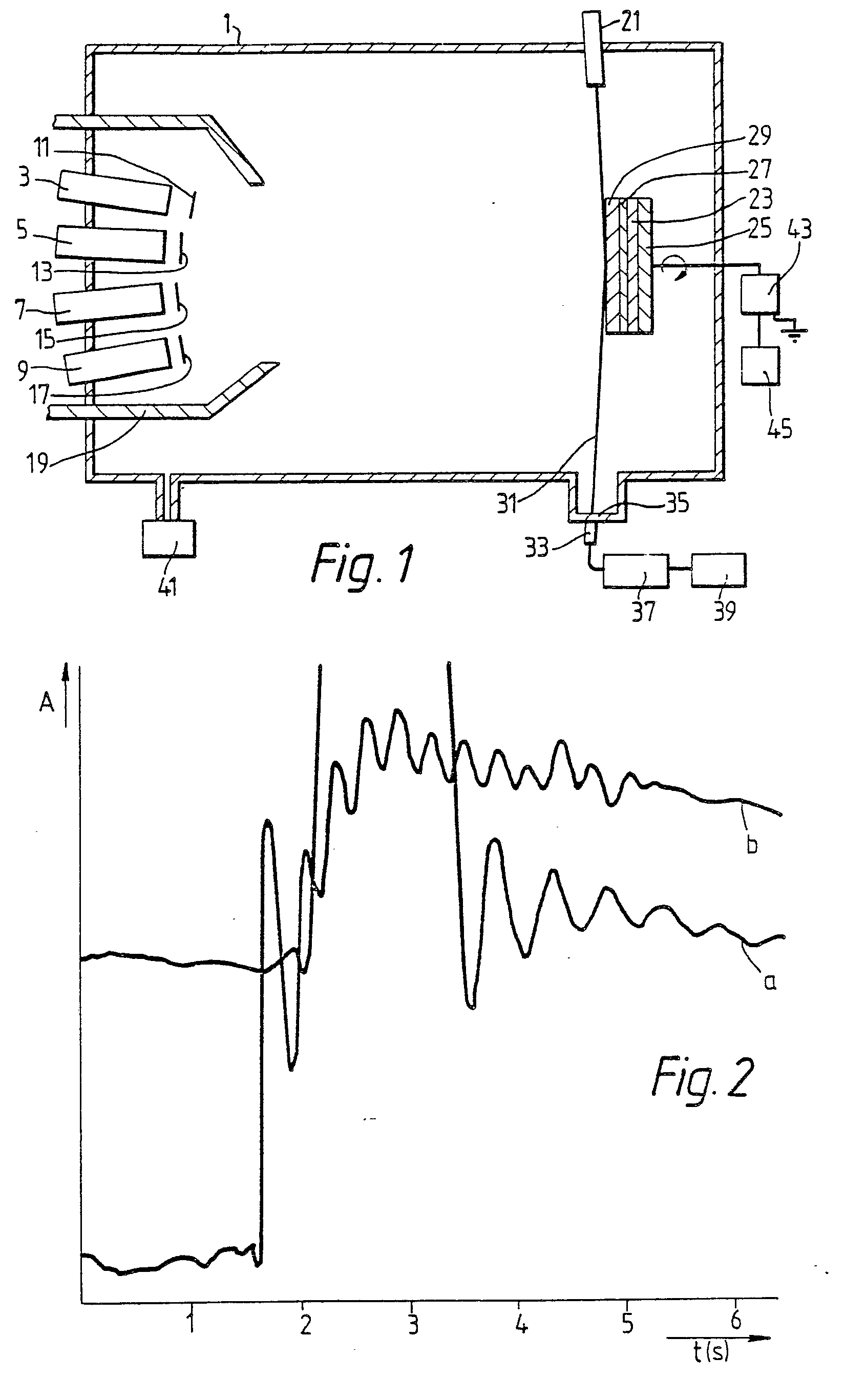
[0022] An embodiment of the invention will now be described with reference to an Example
and to the drawing, in which:-
Figure 1 is a schematic side sectional elevation of a molecular beam epitaxy apparatus
used to perform a method according to the invention, and
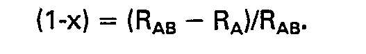
Figure 2 is a graph on which part of a recorder trace of the intensity of a specularly
reflected beam in a RHEED pattern is shown for growth of part of a buffer layer of
GaAs and part of a (Ga,AI)As film grown on this buffer layer.
Example
[0023] Referring to Figure 1, a molecular beam epitaxy apparatus was used comprising a vacuum
chamber 1 provided with effusion cells 3, 5, and 9 each provided with a respective
independently operable shutter 11, 13, 15 and 17, the cells and shutters being disposed
within a shroud 19 cooled by liquid nitrogen. The apparatus includes an electron gun
21 used to irradiate a substrate 23 mounted on a rotatable substrate holder 25, in
order to monitor the substrate cleaning and to determine the growth rate of a GaAs
film 27 grown on the substrate 23 and to determine the growth rate of a (Ga,AI)As
film 29 grown over the GaAs film 27.
[0024] The growth rates were determined by measuring the period of oscillations in the intensity
of a beam 31 of 12 keV electrons which was specularly reflected from the growth surface
on to a reflection electron diffraction screen 35 and photons from the screen 35 were
detected on a photodetector 33. The signals from the photodetector 33 were amplified
by means of an amplifier 37 and were displayed as a trace on a display 39.
[0025] The vacuum chamber 1 was exhausted by means of a pump system 41. The effusion cells
3, 5, 7 and 9 which were loaded with gallium, arsenic, aluminium, and a dopant respectively
were heated to the required temperatures to produce desired fluxes, all the shutters
11, 13, 15 and 17 being closed during this stage. A GaAs substrate 23 was heated to
590°C, and the shutter 13 was opened so that the substrate 23 was exposed to an AS
2 flux of 4 × 10
15 atoms/cm
2/sec. for 20 minutes. The temperature of the substrate 23 was then reduced to 550°C,
and the shutter 11 was then opened so that the substrate 23 was then exposed to a
gallium flux of 1.22 x 10" atoms/cm
2/sec. After a short period (of the order of 10 seconds), a normally reconstructed
surface pattern was observed on the screen 35. The shutter 11 was then momentarily
closed so as to interrupt the gallium flux, and immediately after the gallium flux
was restarted by opening the shutter 11, oscillations in the intensity of the specularly
reflected beam 31 were observed on the display 39. Curve (a) in Figure 2 shows a recorder
trace obtained on the display 39 at this stage. The curve (a) is a plot of the intensity
(measured in arbitrary units) of the specularly reflected beam 31 of electrons with
time t (seconds), and the period of these oscillations is the time of growth of one
monolayer of GaAs which is 0.283 nm (2.83A) thick. After the GaAs film 27 had grown
to a thickness of 100 nm, the shutters 15 and 17 were opened releasing fluxes of 8.7
x 10
14 atoms/cm
2/sec of aluminium and 4.3 x 10
8 atoms/cm
2/sec of the Sn, which fluxes were then incident on the GaAs film 27 and resulted in
the growth of the lightly tin-doped (Ga,AI)As film 29. Immediately after opening the
shutter 15, a curve (b) shown in Figure 2 was observed on the display 39. A monolayer
of (Ga,AI)As is also 0.283 nm (2.83A) thick.
[0026] The results shown in Figure 2 give periods of oscillations during growth of the GaAs
and (Ga,AI)As layers of 0.51 and 0.30 seconds respectively, and these periods correspond
to growth rates of 1.99 um per hour of GaAs and of 3.40 pm per hour of (Ga,AI)As (these
growth rates have an accuracy of ±0.01 pm/hour). Since the lattice constants of GaAs
and AlAs are similar - they only vary by about 1%, the growth rate of (Ga,AI)As is
the arithmetical sum of the growth rates of GaAs and AlAs. Subtracting the GaAs growth
rate from the (Ga,AI)As growth rate gives an AlAs growth rate of 1.41 µm/hour. Thus
the composition of the (Ga,AI)As grown was calculated to be Ga
0.585Al
0,415As. The aluminium fraction of the film 29 was found to be 0.404 when measured by surface
photovoltage, and an ion gauge flux monitor (not shown) used in the growth system
gave an aluminium fraction of 0.405 (these aluminium fractions were accurate to ±0.01).
[0027] Instead of determining the growth rates of the films 27 and 29 by measuring the period
of the oscillations in the intensity of the specularly reflected beam 31, the period
of oscillations in the intensity of the diffracted pattern may be measured when the
photodetector 33 has been moved to an appropriate position on the reflection electron
diffraction screen 35. Alternatively the period of oscillations in the intensity of
the current flowing through the substrate 23 to earth may be measured. The current
is of the order of a few
pA and the amplitude of the oscillations in this current are of the order of a few
tenths of a microampere. A signal derived from this current is amplified by means
of an amplifier 43 and the amplified signals were displayed as a trace on a display
45.
1. A method of growing an alloy film by a layer-by-layer process on a substrate, and
determining the growth rate of the alloy film by irradiating the growing alloy film
with a beam of electrons and measuring the period of oscillations in the intensity
of the stream of electrons diffracted at the growth surface or specularly reflected
by the growth surface, or emitted from the growth surface, or of the current flowing
to earth through the substrate, which period is equal to the growth time of one monolayer
of the alloy on the substrate, characterized in that at least one intermediate film
consisting.of at least one constituent of the alloy is grown between the substrate
and the alloy film, that the growth rate of the/each intermediate film is determined
by irradiating the growing intermediate film with a beam of electrons and measuring
the period of oscillations in the intensity of the stream of electrons diffracted
at the growth surface, specularly reflected by the growth surface, or emitted from
the growth surface, or of the current flowing to earth through the substrate, and
that the atomic ratio of constituents present in the alloy is calculated from the
growth rates of the alloy film and of the intermediate film(s).
2. A method of making a semiconductor device, in which method an alloy film is grown
on a substrate by a layer-by-layer process, and the growth rate of the alloy film
is determined by irradiating the growing alloy film with a beam of electrons and measuring
the period of oscillations in the intensity of the stream of electrons diffracted
at the growth surface or specularly reflected by the growth surface, or emitted from
the growth surface, or of the current flowing to earth through the substrate, which
period is equal to the growth time of one monolayer of the alloy on the substrate,
characterized in that at least one intermediate film of at least one constituent of
the alloy is grown between the substrate and the alloy film, that the growth rate
of the/each intermediate film is determined by irradiating the growing intermediate
film with a beam of electrons and measuring the period of oscillations in the intensity
of the stream of electrons diffracted at the growth surface, specularly reflected
by the growth surface, or emitted from the growth surface, or of the current flowing
to earth through the substrate, and that the atomic ratio of constituents present
in the alloy is calculated from the growth rates of the alloy film and of the intermediate
film(s).
3. A method according to Claim 1 or Claim 2, characterized in that the layer-by-layer
process is a molecular beam epitaxy process.
4. A method according to any preceding Claim, characterized in that the alloy is a
ternary III-V alloy ABC in which the "elements A and C are group III elements, and that the method comprises the steps of
growing a buffer layer of the compound AB on the substrate and determining the growth
rate of the buffer layer, growing the film of the alloy ABC by continuing to supply
the species A and B to the growth surface without changing the conditions of the sources
supplying the species A and B and additionally supplying species C to the growth surface,
determining the growth rate of the film of the alloy ABC, calculating the growth rate
of the constituent BC of the alloy ABC by subtracting the growth rate of the buffer
layer AB from the growth rate of the alloy film ABC, and calculating the ratio of
the growth rate of the compound AB to the growth rate of the constituent BC, which
ratio is equal to the atomic ratio A:C in the alloy film ABC.
5. A method according to any of claims 1-3, characterized in that the alloy is a quaternary
III-V alloy ABCD in which the elements A and B belong to different groups and elements
A, C and D belong to group III, and that the method comprises the steps of growing
a buffer layer of a compound AB on the substrate and determining the growth rate of
the buffer layer, growing a film of an alloy ABC on the buffer layer by continuing
to supply species A and B to the growth surface without changing the conditions of
the sources supplying the species A and B and additionally supplying species C to
the growth surface, determining the growth rate of the film of the alloy ABC, growing
a film of the alloy ABCD on the alloy film ABC by continuing to supply species A,
B and C to the growth surface without changing the conditions of the sources A, B
and C and additionally supplying species D to the growth surface, and determining
the growth rate of the film of the alloy ABCD, calculating the growth rates of the
compounds BC and BD by subtracting the growth rates of the buffer layer and of the
film ABC from the growth rates of the films ABC and ABCD respectively, and calculating
the ratios of the growth rate of the buffer layer to the growth rate of the compound
BC to the growth rate of the compound BD, which ratios are equal to the ratios of
the atomic ratios A:C:D in the alloy film ABCD.
6. A method according to any of claims 1-3, characterized in that the alloy is a quaternary
III-V alloy ABCD in which elements A and C belong to group III and elements B and
D belong to group V, and that the method comprises the steps of growing a buffer layer
of a compound AB on the substrate and determining the growth rate of the buffer layer,
growing a film of the alloy ABCD on the buffer layer AB by continuing to supply the
species A and B to the growth surface without changing the conditions of the sources
of A and B and additionally supplying species C and D to the growth surface, measuring
the growth rate of the film ABCD, calculating the growth rate of a compound CD by
subtracting the growth rate of the buffer layer AB from the growth rate of the film
ABCD, and calculating the ratio of the growth rate of the compound AB to the growth
rate of the compound CD, which ratio is equal to the atomic ratio A:C in the alloy
film ABCD.
7. A method according to any of claims 1-3, characterized in that the alloy is a ternary
II-VI or IV-VI alloy ABC in which the elements A and C belong to the same group of
the periodic table, and that the method comprises the steps of growing a film of A
on the substrate and determining the growth rate of the film A, growing a film of
a compound AB on the film A by continuing to supply species A to the growth surface
without changing the conditions of the source supplying the species A and additionally
supplying species B to the growth surface, determining the growth rate of the film
AB, growing a film of the alloy ABC on the film of the alloy AB by continuing to supply
the species A and B to the growth surface without changing the conditions of the sources
supplying the species A and B and additionally supplying species C to the growth surface,
determining the growth rate of the film of the alloy ABC, calculating the growth rate
of the constituents B and C by subtracting the growth rate of the films of A and AB
from the growth rates of the films AB and ABC respectively, and calculating the ratios
of the growth rates of the constituents A:B:C, which ratios are equal to the atomic
ratios A:B:C in the alloy ABC.
8. A method according to any of claims 1-3, characterized in that the alloy is a quaternary
alloy ABCD which is a quaternary II-VI or, IV-VI alloy, in which alloy elements A
and B belong to different groups of the periodic table, and that the method comprises
the steps of growing a film of A on the substrate and determining the growth rate
of the film A, growing a film of a compound AB on the film A by continuing the supply
species A to the growth surface without changing the conditions of the source supplying
the species A and additionally supplying species B to the growth surface, measuring
the growth rate of the film AB, growing a film of an alloy ABC on the film AB by continuing
to supply species A and B to the growth surface without changing the conditions of
the sources supplying the species A and B and additionally supplying species C to
the growth surface, determining the growth rate of the film of the alloy ABC, growing
a film of the alloy ABCD on the alloy film ABC by continuing to supply species A,
B and C to the growth surface without changing the conditions of the sources A, B
and C and additionally supplying species D to the growth surface, and determining
the growth rate of the film of the alloy ABCD, calculating the growth rates of the
constituents B, C and D by subtracting the growth rates of the films A, AB and ABC
from the growth rates of the films AB, ABC and ABCD respectively, and calculating
the ratios of the growth rates of the constituents A:B:C:D, which ratios are equal
to the atomic ratios A:B:C:D in the alloy ABCD.
9. A method according to any preceding Claim, in which the layer-by-layer process
is controlled by control means, characterized in that the input signals derived from
the oscillations in the intensity of the stream of electrons diffracted at or specularly
reflected by, or emitted from the growth surface, or flowing to earth through the
substrate are fed into the control means, which input signals are compared by the
control means with preset signals corresponding to a desired alloy composition, and
that the control means adjust the operation of sources of constituent elements of
the alloy supplying these elements to the alloy film growth surface until the input
signals correspond to the preset signals.
10. A method according to Claim 1, characterized in that the layer-by-layer process
is a vacuum evaporation process.
11. A method according to Claim 1 or Claim 10, characterized in that the alloy is
a binary alloy ABC, and that the method comprises the steps of growing a buffer layer
of A on the substrate and determining the growth rate of the buffer layer, growing
a film of the alloy AB on the buffer layer by continuing to deposit A on the growth
surface without changing the conditions of the source supplying A and additionally
depositing constituent B of the alloy on the growth surface, determining the growth
rate of the alloy AB film, and calculating the ratio of the growth rate of the buffer
layer to the growth rate of the alloy film, which ratio is equal to the atomic fraction
of A present in the alloy AB.
1. Verfahren zum schichtweisen Auftragen eines Legierungsfilmes auf ein Substrat und
zum Bestimmen der Wachstumsgeschwindigkeit des Legierungsfilmes durch Anstrahlen des
wachsenden Legierungsfilmes mit einem Elektronenstrahl und zum Messen der Schwingungsdauer
in der Intensität des an der Wachstumsoberfläche abgebeugten oder von der Wachstumsoberfläche spiegelnd zurückgeworfenen oder von der Wachstumsoberfläche ausgestrahlten Elektronenstroms
oder des das Substrat durchfliessenden und nach Erde abfliessenden Stroms, wobei diese
Dauer gleich der Wachstumszeit einer einzigen Monoschicht der Legierung auf dem Substrat
ist, dadurch gekennzeichnet, dass zumindest ein Zwischenfilm, der aus mindestens einem
Bestandteil der Legierung besteht, zwischen dem Substrat und dem Legierungsfilm gezüchtet
wird, dass die Wachstumsgeschwindigkeit des Zwischenfilms oder jedes Zwischenfilms
durch Anstrahlung des wachsenden Zwischenfilms mit einem Elektronenstrahl bestimmt
und durch Messung der Schwingungsdauer in der Intensität des an der Wachstumsoberfläche
abgebeugten, von der Wachstumsoberfläche spiegelnd zurückgeworfenen oder von der Wachstumsoberfläche
ausgestrahlten Elektronenstroms oder des das Substrat nach Erde durchfliessenden Stroms
bestimmt wird, und dass das Atomverhältnis von in der Legierung vorhandenen Bestandteilen
aus den Wachstumsgeschwindigkeiten des Legierungsfilms und des bzw. der Zwischenfilm(e)
errechnet wird.
2. Verfahren zum Herstellen einer Halbleitervorrichtung, bei dem ein Legierungsfilm
auf einem Substrat durch schichtweise Auftragen gezüchtet wird und die Wachstumsgeschwindigkeit
des Legierungsfilms durch Anstrahlen des wachsenden Legierungsfilms mit einem Elektronenstrahl
und durch Messung der Schwingungsdauer in der Intensität des an der Wachstumsoberfläche
abgebeugten oder spiegelnd von der Wachstumsoberfläche zurückgeworfenen oder von der
Wachstumsoberfläche ausgestrahlten Elektronstromes oder des das Substrat nach Erde
durchfliessenden Stroms bestimmt wird, wobei die Dauer gleich der Wachstumszeit einer
Einzelschicht der Legierung auf dem Substrat ist, dadurch gekennzeichnet, dass mindestens
ein Zwischenfilm mindestens eines Legierungs-Bestandteils zwischen dem Substrat und
dem Legierungsfilm gezüchtet wird, dass die Wachstumsgeschwindigkeit des Zwischenfilmes
oder jedes Zwischenfilmes durch Anstrahlen des wachsenden Zwischenfilms mit einem
Elektronenstrahl und durch Messung der Schwingungsdauer in der Intensität des an der
Wachstumsoberfläche abgebeugten spiegelnd von der Wachstumsoberfläche zurückgeworfenen
oder von der Wachstumsoberfläche ausgestrahlten Elektronenstroms oder des das Substrat
nach Erde durchfliessenden Stroms bestimmt wird, und dass das Atomverhältnis der in
der Legierung vorhandenen Bestandteile aus den Wachstumsgeschwindigkeiten des Legierungsfilms
und des bzw. der Zwischenfilm(e) errechnet wird.
3. Verfahren nach Anspruch 1 oder 2, dadurch gekennzeichnet, dass das schichtweise
Verfahren ein molekulares Strahlepitaxieverfahren ist.
4. Verfahren nach einem der vorangehenden Ansprüche, dadurch gekennzeichnet, dass
die Legierung eine ternäre III-V-Legierung ABC ist, in der die Elemente A und C Gruppe-III-Elemente
sind, und dass das Verfahren die Schritten zum Züchten einer Pufferschicht der Verbindung
AB auf dem Substrat und zum Bestimmen der Wachstumsgeschwindigkeit der Pufferschicht,
zum Züchten des Films der Legierung ABC durch fortgesetztes Zuführen der Arten A und
B zur Wachstumsoberfläche ohen Änderung der Bedingungen der die Arten A und B liefernden
Quellen und zum zusätzlichen Zuführen der Art C zur Wachstumsoberfläche, zum Bestimmen
der Wachstumsgeschwindigkeit des Filmes der Legierung ABC, zum Berechnen der Wachstumsgeschwindigkeit
des Bestandteils BC der Legierung ABC durch Substraktion der Wachstumsgeschwindigkeit
der Pufferschicht AB von der Wachstumsgeschwindigkeit des Legierungsfilms ABC und
zum Berechnen des Verhältnisses der Wachstumsgeschwindigkeit der Verbindung AB zur
Wachstumsgeschwindigkeit des Bestandteils BC enthält, und dieses Verhältnis gleich
dem Atomverhältnis A:C im Legierungsfilm ABC ist.
5. Verfahren nach einem der Ansprüche 1 bis 3, dadurch gekennzeichnet, dass die Legierung
eine quaternäre 111-V-Legierung ABCD ist, in der Elemente A und B zu verschiedenen
Gruppen und Elemente A, C und D zur Gruppe 111 gehören, und dass das Verfahren die
Schritte zum Züchten einer Pufferschicht einer Verbindung AB auf dem Substrat und
zum Bestimmen der Wachstumsgeschwindigkeit der Pufferschicht, zum Züchten eines Filmes
einer Legierung ABC auf der Pufferschicht durch fortgesetztes Zuführen der Arten A
und B zur Wachstumsoberfläche ohne Änderung - der Bedingungen der die Arten A und
B liefernden Quellen und zum zusätzlichen Versorgen der Art C zur Wachstumsoberfläche,
zum Bestimmen der Wachstumsgeschwindigkeit des Filmes der Legierung ABC, zum Züchten
eines Filmes der Legierung ABCD auf dem Legierungsfilm ABC durch fortgesetztes Zuführen
der Arten A B und C zur Wachstumsoberfläche ohne Änderung der Bedingungen der Quellen
A, B und C und zum zusätzlichen Zuführen der Art D zur Wachstumsoberfläche und zum
Bestimmen der Wachstumsgeschwindigkeit des Filmes der Legierung ABCD, zum Errechnen
der Wachstumsgeschwindigkeiten der Verbindungen BC und BD durch Subtraktion der Wachstumsgeschwindigkeiten
der Pufferschicht und des Filmes ABC von den Wachstumsgeschwindigkeiten der filme
ABC bzw. ABCD und zum Berechnen der Verhältnisse der Wachstumsgeschwindigkeit der
Pufferschicht zur Wachstumsgeschwindigkeit der Verbindung BC zur Wachstumsgeschwindigkeit
der Verbindung BD enthält, und diese Verhältnisse gleich den Verhältnissen der Atomverhältnisse
A:C:D im Legierungsfilm ABCD sind.
6. Verfahren nach einem der vorangehenden Ansprüche 1 bis 3, dadurch gekennzeichnet,
dass die Legierung eine quaternäre III-V-Legierung ABCD ist, in der Elemente A und
C zur Gruppe 111 und Elemente B und D zur Gruppe V gehören, und dass das Verfahren
die Schritte zum Züchten einer Pufferschicht einer Verbindung AB auf dem Substrat
und zum Bestimmen der Wachstumsgeschwindigkeit der Pufferschicht, zum Züchten eines
Filmes der Legierung ABCD auf der Pufferschicht AB durch fortgesetztes Zuführen der
Arten A und B zur Wachstumsoberfläche ohne Änderung der Bedingungen der Quellen von
A und B und zum zusätzlichen Zuführen der Arten C und D zur Wachstumsoberfläche, zum
Messen der Wachstumsgeschwindigkeit des Filmes ABCD, zum Berechnen der Wachstumsgeschwindigkeit
einer Verbindung CD durch Subtraktion der Wachstumsgeschwindigkeit der Pufferschicht
AB von der Wachstumsgeschwindigkeit des Filmes ABCD und zum Errechnen des Verhältnisses
der Wachstumsgeschwindigkeit der Verbindung AB zur Wachstumsgeschwindigkeit der Verbindung
CD enthält, und dieses Verhältnis gleich dem Atomverhältnis A:C im Legierungsfilm
ABCD ist.
7. Verfahren nach einem der vorangehenden Ansprüche 1 bis 3, dadurch gekennzeichnet,
dass die Legierung eine quaternäre II-VI- oder IV-VI-Legierung ABC ist, in der die
Elemente A und C zur gleichen Gruppe der periodischen Tabelle gehören, und dass das
Verfahren die Schritte zum Züchten eines Filmes von A auf dem Substrat und zum Bestimmen
der Wachstumsgeschwindigkeit des Filmes A, zum Züchten eines Filmes einer Verbindung
AB auf dem Film A durch fortgesetztes Zuführen der Art Z zur Wachstumsoberfläche ohne
Änderung der Bedingungen der die Art A liefernden Quelle und zum zusätzlichen Zuführen
der Art B zur Wachstumsoberfläche, zum Bestimmen der Wachstumsgeschwindigkeit des
Filmes AB, zum Züchten eines Filmes der Legierung ABC auf der Film der Legierung AB
durch fortgesetztes Zuführen der Arten A und B zur Wachstumsoberfläche ohne Änderung
der Bedingungen der die Arten A und B liefernden Quellen und zum zusätzlichen Zuführen
der Art C zur Wachstumsoberfläche, zum Bestimmen der Wachstumsgeschwindigkeit des
Filmes der Legierung ABC, zum Errechnen der Wachstumsgeschwindigkeit der Bestandteile
B und C durch Subtraktion der Wachstumsgeschwindigkeit der Filme A und AB von den
Wachstumsgeschwindigkeiten der Filme AB bzw. ABC, und zum Errechnen der Verhältnisse
der Wachstumsgeschwindigkeiten der Bestandteil A:B:C enthält, und diese Verhältnisse
gleich den Atomverhältnissen A:B:C in der Legierung ABC sind.
8. Verfahren nach einem der vorangehenden Ansprüche 1 bis 3, dadurch gekennzeichnet,
dass die Legierung eine quaternäre Legierung ABCD ist, die eine quaternäre II-VI-
oder IV-VI-Legierung ist, in der Legierungselemente A und B zu verschiedenen Gruppen
der periodischen Tabelle gehören und dass das Verfahren die Schritte zum Züchten eines
Filmes von A auf dem Substrat und zum Bestimmen der Wachstumsgeschwindigkeit des Filmes
A, zum Züchten eines Filmes einer Verbindung AB auf dem Film A durch fortgesetztes
Zuführen der Art A zur Wachstumsoberfläche ohne Änderung der Bedingungen der die Art
A liefernden Quelle und zum zusätzlichen Zuführen der Art B zur Wachstumsoberfläche,
zum Messen der Wachstumsgeschwindigkeit des Filmes AB, zum Züchten eines Filmes einer
Legierung ABC auf dem Film AB durch fortgesetztes Zuführen der Arten A und B zur Wachstumsoberfläche
ohne Änderung der Bedingungen der die Arten A und B liefernden Quellen und zum zusätzlichen
Zuführen der Art C zur Wachstumsoberfläche, zum Bestimmen der Wachstumsgeschwindigkeit
des Filmes der Legierung ABC, zum Züchten eines Filmes der Legierung ABCD auf dem
Legierungsfilm ABC durch fortgesetztes Zuführen der Arten A, B und C zur Wachstumsoberfläche
ohne Änderung der Bedingungen der Quellen A, B und C und zum zusätzlichen Zuführen
der Art D zur Wachstumsoberfläche und zum Bestimmen der Wachstumsgeschwindigkeit des
Films der Legierung ABCD, zum Errechnen der Wachstumsgeschwindigkeiten der Bestandteile
B, C und D durch Subtraktion der Wachstumsgeschwindigkeiten der Filme A, AB und ABC
von den Wachstumsgeschwindigkeiten der Filme AB, ABC bzw. ABCD und zum Errechnen der
Verhältnisse der Wachstumsgeschwindigkeiten der.Bestandteile A:B:C:D enthält, und
diese Verhältnisse gleich den Atomverhältnissen A:B:C:D: in der Legierung ABCD sind.
9. Verfahren nach einem oder mehreren der vorangehenden Ansprüche, in dem das schichtweise
Auftragen durch Steuermittel gesteuert wird, dadurch gekennzeichnet, dass Eingangssignale
aus den Schwingungen in der Intensität des an der Wachstumsoberfläche abgebeugten
oder spiegelnd von der Wachstumsoberfläche zurückgeworfenen oder von der Wachstumsoberfläche
ausgestrahlten Elektronenstromes oder des das Substrat nach Erde durchfliessenden
Stromes in die Steuermittel eingegeben werden, und diese Eingangssignale durch die
Steuermittel mit Voreinstellsignale entsprechend einer gewünschten Legierungszusammensetzung
verglichen werden, und dass die Steuermittel den Betrieb der Quellen der zusammenstellenden
Elemente der Legierung einstellen, und diese Quellen die Wachstumsoberfläche des Legierungsfilms
mit diesen Elementen beliefern, bis die Eingangssignale den Voreinstellsignalen entsprechen.
10. Verfahren nach Anspruch 1, dadurch gekennzeichnet, dass das schichtweise Auftragen
ein Vakuumverdampfungsverfahren darstellt.
11. Verfahren nach Anspruch 1 oder 10, dadurch gekennzeichnet, dass die Legierung
eine Binärlegierung AB ist, und dass das Verfahren die Schritte zum Züchten einer
Pufferschicht von A auf dem Substrat und zum Bestimmen der Wachstumsgeschwindigkeit
der Pufferschicht, zum Züchten eines Filmes der Legierung AB auf der Pufferschicht
durch fortgesetztes Ablagern von A auf der Wachstumsoberfläche ohne Änderung der Bedingungen
der A liefernden Quelle und zum zusätzlichen Ablagern des Bestandteils B der Legierung
auf der Wachstumsoberfläche, zum Bestimmen der Wachstumsgeschwindigkeit des AB-Legierungsfilms
und zum Errechnen der Verhältnisses der Wachstumsgeschwindigkeit der Pufferschicht
zur Wachstumsgeschwindigkeit des Legierungsfilms enthält, und dieses Verhältnis gleich
dem Atombruchteil von A in der Legierung AB ist.
1. Procédé de croissance d'un film d'alliage sur un substrat par un processus couche
par couche et de détermination de la vitesse de croissance du film par irradiation
du film d'alliage en cours de croissance au moyen d'un faisceau électronique et par
mesure du temps d'oscillation dans l'intensité soit du flux d'électrons diffracté
sur la surface de croissance ou réfléchi de façon spéculaire ou émis par la surface
de croissance, soit du courant circulant. vers la masse à travers le substrat, temps
qui est égal au temps de croissance d'une monocouche d'alliage sur le substrat, caractérisé
en ce qu'on fait croître entre le substrat et le film d'alliage, au moins un film
intermédiaire consistant en au moins un constituant de l'alliage.en ce que la vitesse
de croissance du film intermédiaire ou de chaque film intermédiaire est déterminée
par irradiation du film intermédiaire en cours de croissance au moyen d'un faisceau
d'électrons et par mesure de la période d'oscillation dans l'intensité, soit du flux
d'électrons diffracté sur la surface de croissance ou réfléchi de façon spéculaire
ou émis par la surface de croissance, soit du courant circulant vers la masse à travers
le substrat, et en ce que le rapport atomique de constituants présents dans l'alliage
est calculé à partir des vitesses de croissance du film d'alliage et du (des) film(s)
intermédiaire(s).
2. Procédé de fabrication d'un dispositif semiconducteur, suivant lequel on fait croître
un film d'alliage sur un substrat par un processus couche par couche et on détermine
la vitesse de croissance du film d'alliage par irradiation du film d'alliage en cours
de croissance au moyen d'un faisceau d'électrons et par mesure de temps d'oscillation
dans l'intensité soit du flux d'électrons diffracté sur la surface de croissance ou
réfléchi de façon spéculaire ou émis par la surface de croissance, soit du courant
circulant vers la masse à travers le substrat, temps qui est égal au temps de croissance
d'une monocouche d'alliage sur le substrat, caractérisé en ce qu'on fait croître entre
le substrat et le film d'alliage, au moins un film intermédiaire consistant en au
moins un constituant de l'alliage en ce que la vitesse de croissance du film intermédiaire
ou de chaque film intermédiaire est déterminée par irradiation du film intermédiaire
en cours de croissance au moyen d'un faisceau d'électrons et par mesure du temps d'oscillation
dans l'intensité soit du flux d'électrons diffracté sur la surface de croissance ou
réfléchi de façon spéculaire ou émis par la surface de croissance, soit du courant
circulant vers la masse à travers le substrat, et en ce que le rapport atomique de
constituants présents dans l'alliage est calculé à partir des vitesses de croissance
du film de l'alliage et du (des) film(s) intermédiaire(s).
3. Procédé selon la revendication 1 ou 2, caractérisé en ce que le processus couche
par couche est un processus d'épitaxie à faisceau moléculaire.
4. Procédé selon l'une quelconque des revendications précédentes, caractérisé en ce
que l'alliage est un alliage III-V ternaire ABC dans lequel les éléments A et C sont
des éléments du groupe III et en ce que le procédé comporte les étapes de croissance
sur le substrat d'une couche tampon constitué par le composé AB et de détermination
de la vitesse de croissance de la couche tampon, de croissance du film d'alliage ABC
en continuant à fournir les éléments A et B à la surface de croissance sans changer
les conditions des sources fournissant les éléments A et B ainsi que l'élément C à
la surface de croissance, de détermination de la vitesse de croissance du film d'alliage
ABC, de calcul de la vitesse de croissance du constituant BC de l'alliage ABC par
soustraction de la vitesse de croissance de la couche tampon AB de la vitesse de croissance
du film d'alliage ABC, et de calcul du rapport de la vitesse de croissance du composé
AB à la vitesse de croissance du constituant BC, rapport qui est égal au rapport atomique
A:C dans le film d'alliage ABC.
5. Procédé selon l'une des revendications 1 à 3, caractérisé en ce que l'alliage est
un alliage III-V quaternaire ABCD dans lequel les éléments A et B appartiennent à
des groupes différents et les éléments A, C et D appartiennent au groupe III et en
ce que le procédé comporte les étapes de croissance sur le substrat d'une couche tampon
constitué par le composé AB et de détermination de la vitesse de croissance de la
couche tampon, de croissance d'un film d'alliage ABC sur la couche tampon en continuant
à fournir les éléments A et B à la surface de croissance sans changer les conditions
des sources fournissant les éléments A et B ainsi que l'élément C à la surface de
croissance, de détermination de la vitesse de croissance du film d'alliage ABC, de
croissance d'un film d'alliage ABCD sur le film d'alliage ABC en continuant à fournir
les éléments A, B et C à la surface de croissance sans changer les conditions des
sources A, B et C et en fournissant en outre l'élément D à la surface de croissance,
de détermination de la vitesse de croissance du film d'alliage ABCD, de calcul des
vitesses de croissance des composés BC et BD par soustraction des vitesses de croissance
de la couche tampon et du film ABC respectivement des vitesses de croissance des films
ABC et ABCD, et de calcul des rapports de la vitesse de croissance de la couche tampon
à la vitesse de croissance du composé BC à la vitesse de croissance du composé BD,
rapports qui sont égaux aux rapports des rapports atomiques A:C:D dans le film d'alliage
ABCD.
6. Procédé selon l'une quelconque des revendications 1 à 3, caractérisé en ce que
l'alliage est un alliage III-V quaternaire ABCD dans lequel les éléments A et C appartiennent
au groupe III et les éléments B et D appartiennent au groupe V et en ce que le procédé
comporte les étapes de croissance sur le substrat d'une couche tampon constituée par
un composé AB et de détermination de la vitesse de croissance de la couche tampon,
de croissance d'un film d'alliage ABCD sur la couche tampon AB en continuant à fournir
les éléments A et B à la surface de croissance sans changer les conditions des sources
de A et de B et en fournissant en outre les éléments C et D à la surface de croissance,
de mesure de la vitesse de croissance du film ABCD, de calcul de la vitesse de croissance
d'un composé CD par soustraction de la vitesse de croissance de la couche tampon AB
de la vitesse de croissance du film ABCD, et de calcul du rapport de la vitesse de
croissance du composé AB à la vitesse de croissance du composé CD, rapport qui est
égal au rapport atomique A:C dans le film d'alliage ABCD.
7. Procédé selon l'une quelconque des revendications 1 à 3, caractérisé en ce que
l'alliage est un alliage II-VI ou IV-VI ternaire ABC dans lequel les éléments A et
C appartiennent au même groupe de la table périodique, et en ce que le procédé comporte
les étapes de croissance d'un film de A sur le substrat et de détermination de la
vitesse de croissance du film A, de croissance sur le film A d'un film constitué par
un composé AB en continuant à fournir l'élément A à la surface de croissance sans
changer les conditions de la source fournissant l'élément A et un fournissant en outre
l'élément B à la surface de croissance, de . détermination de la vitesse de croissance
du film AB, de croissance d'un film d'alliage ABC sur le film d'alliage AB en continuant
à fournir les éléments A et B à la surface de croissance sans changer les conditions
des sources fournissant les éléments A et B et en fournissant en outre l'élément C
à la surface de croissance, de détermination de la vitesse de croissance du film d'alliage
ABC, de calcul de la vitesse de croissance des constituants B et C par soustraction
des vitesses de croissance des films de A et de AB respectivement des vitesses de
croissance des films AB et ABC, et de calcul des rapports des vitesses de croissance
des constituants A:B:C, rapports qui sont égaux aux rapports atomiques A:B:C dans
l'alliage ABC.
8. Procédé selon l'une quelconque des revendications 1 à 3, caractérisé en ce que
l'alliage est un alliage ABCD quaternaire qui est un alliage II-VI ou IV-VI quaternaire
dans lequel les éléments d'alliage A et B appartiennent à des groupes différents de
la table périodique et en ce que le procédé comporte les étapes de croissance d'un
film de A sur le substrat et de détermination de la vitesse de croissance du film
A, de croissance, sur le film A, d'un film constitué par un composé AB en continuant
à fournir l'élément A à la surface de croissance sans changer les conditions de la
source fournissant l'élément A et en fournissant en outre l'élément B à la surface
de croissance, de détermination de la vitesse de croissance du film AB, de croissance
d'un film d'alliage ABC sur le film AB et continuant à fournir les éléments A et B
à la surface de croissance sans changer les conditions des sources fournissant les
éléments A et B et en fournissant en outre l'élément C à la surface de croissance,
de détermination de la vitesse de croissance du film d'alliage ABC, de croissance
d'un film d'alliage ABCD sur le film d'alliage ABC en continuant à fournir les éléments
A, B et C à la surface de croissance sans changer les conditions des sources A, B
et C et en fournissant en outre les éléments D à la surface de croissance, et de détermination
de la vitesse de croissance du film d'alliage ABCD, de calcul des vitesses de croissance
des constituants B, C et D par soustraction des vitesses de croissance des films A,
AB et ABC respectivement des vitesses de croissance des films AB, ABC et ABCD, et
de calcul des rapports des vitesses de croissance des constituants A:B:C:D, rapports
qui sont égaux aux rapports atomiques A:B:C:D dans l'alliage ABCD.
9. Procédé selon l'une quelconque des revendications précédentes, dans lequel le processus
couche par couche est commandé par des moyens de commande, caractérisé en ce que les
moyens de commande reçoivent des signaux d'entrée déduits des oscillations dans l'intensité
soit du flux d'électrons diffracté sur la surface de croissance ou refléchi de façon
spéculaire ou émis par la surface de croissance, soit du courant circulant vers la
masse à travers le substrat, signaux d'entrée qui sont comparés par les moyens de
commande avec des signaux préréglés correspondant à une composition d'alliage souhaitée
et en ce que les moyens de commande ajustent le fonctionnement de sources d'éléments
constituants de l'alliage fournissant ces éléments à la surface de croissance du film
d'alliage jusqu'à ce que les signaux d'entrée correspondent aux signaux préréglés.
10. Procédé selon la revendication 1, caractérisé en ce que le processus couche par
couche est un processus d'évaporation sous vide.
11. Procédé selon la revendication 1 ou la revendication 10, caractérisé en ce que
l'alliage est un alliage binaire AB et en ce que le procédé comporte les étapes de
croissance d'une couche tampon de A sur le substrat et de détermination de la vitesse
de croissance de la couche tampon, de croissance d'un film d'alliage AB sur la couche
tampon en continuant à déposer A sur la surfacer- de croissance sans changer les conditions
de la source fournissant A et en déposant en outre le constituant B de l'alliage sur
la surface de croissance, de détermination de la vitesse de croissance du film d'alliage
AB et de calcul du rapport de la vitesse de croissance de la couche tampon à la vitesse
de croissance du film d'alliage, rapport qui est égal à la fraction atomique de A
présente dans l'alliage AB.