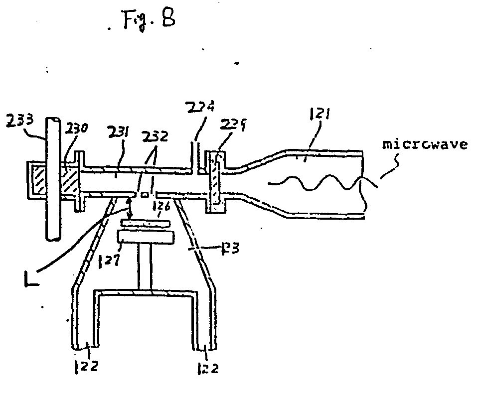
(57) @ A plasma processing device for dry etching or ashing has a plasma generation region
(131. 231), constituted within a waveguide (121) through which microwave power is
transmitted, into which a reactive gas is introduced and a plasma generated by the
microwave power applied thereto, and a reaction region (123) adjoined to the plasma
generation region (131,231) by way of a shielding means (125,232) through which radicals
of the reactive gas generated in the plasma enter the reaction region (123) while
microwaves and plasma are prevented from entering the reaction region (123). Dielectric
means divide the plasma generation region (131, 231) from the remainder of the waveguide
(121).
|
|
