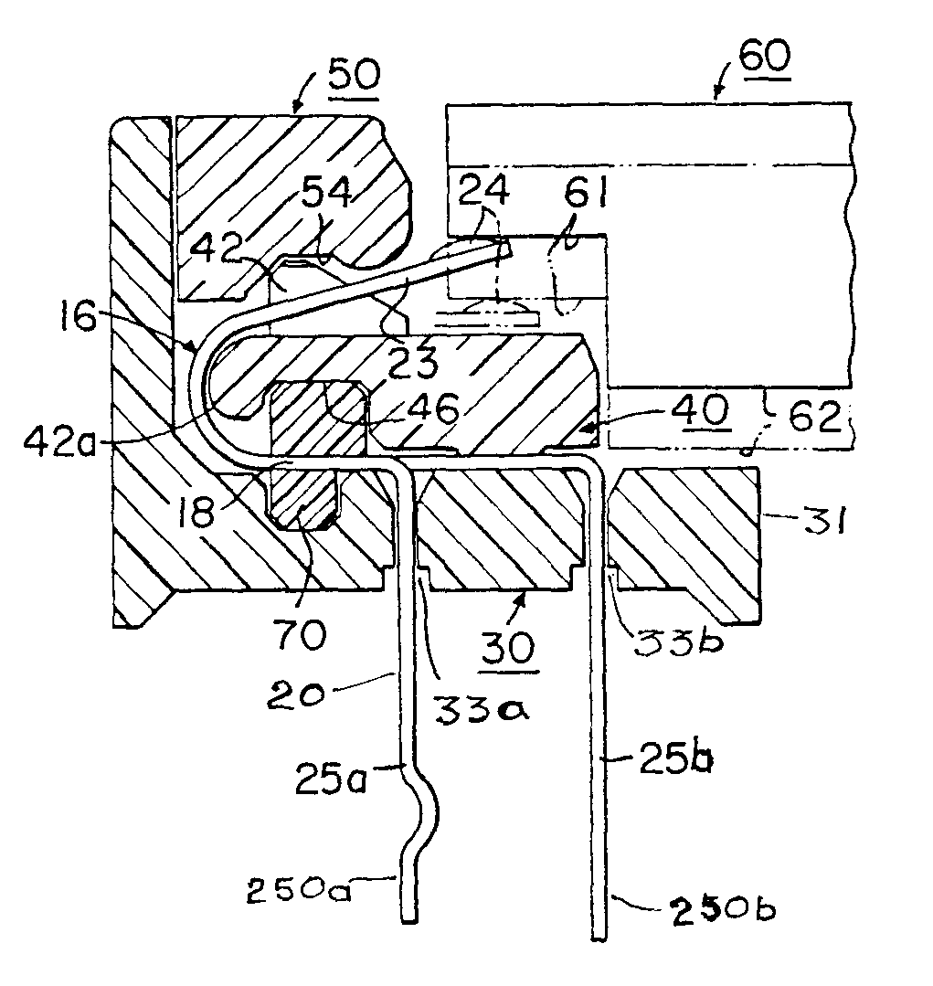
(57) An electrical connector for connecting electrode members of a chip carrier (60) to
circuit paths of a circuit board comprises a base housing (30) having rows of aligned
apertures (33a, 33b) extending through a bottom section (31) of housing (30). A contact
assembly (20, 40) has electrical contacts (16) which include spring contact portions
(23) for electrical engagement with respective electrode members of chip carrier (60)
and inclined and aligned terminal portions (25a, 25b) in rows (250A, 250B) that are
disposed in respective apertures (33a, 33b) for electrical connection with respective
circuit paths of the circuit board and a depressing member on the base housing (30)
that depresses the electrode members of the chip carrier (60) into wiping electrical
contact with the contact portions (23).
|
|
