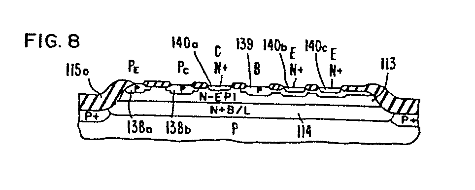
(57) A semiconductor structure is fabricated using a process involving all ion implantation
and using only five masks prior to metallization. A buried contact mask is used to
form a buried contact layer (114), an isolation mask is used to form grooves (130a,
130b) in an epitaxial layer of silicon (113), a self-aligned transistor mask is used
to form a mask (134a to 134e) to define the areas in which emitters (138a, 140b, 140c)
bases (113,139) and contact regions (140a) are to be formed, a base exclusion mask
(135a,b) is provided to exclude certain impurities from being implanted into a region
to be formed of one conductivity type, and a second exclusion mask (137a, 137b) is
provided to exclude impurities to be implanted in a region of opposite conductivity
type from the prohibited regions of the structure. The last ion implantation of the
device is a two-level implantation to yield a shallow implant which provides good
ohmic contact to certain to-be-formed metal contact areas and a deep implant to provide
current gain control for the base of the NPN transistors (Qi, Q2). The metal contacts to active regions on the device are formed merely by etching
the device to remove a thin oxide (131) over these regions. A thicker oxide (134a
through 134e) overlying all other regions of the device is substantially unaffected
by this etching.
|
|
