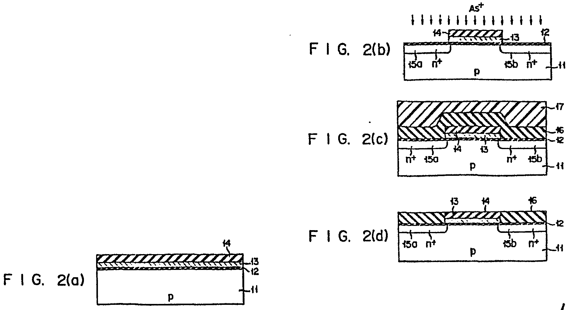
(57) A method for manufacturing a semiconductor device, comprises the steps of sequentially
forming a gate insulation film (12), a gate electrode film (13) of polycrystalline
silicon and a self-alignment film (14) of silicon nitride on a semiconductor substrate
(11) having one conductivity type, patterning the gate electrode film (13) and the
self-alignment film (14) in an identical electrode pattern, ion-implanting an impurity
of an opposite conductivity type into the substrate (11) using the silicon nitride
pattern (14) as a mask, thereby forming source and drain regions (15a, 15b), forming
an insulation layer (16) on the entire surface of the substrate (11) including the
silicon nitride pattern (14), performing annealing, removing the remaining insulation
layer (16) which is located on the silicon nitride pattern (14), removing the silicon
nitride pattern (14) so as to expose the gate electrode pattern (13), and forming
a metal film (18) on the exposed gate electrode pattern (13).
|
|
