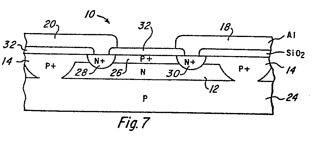
(57) A semiconductor Hall effect device having a stable and more controllable offset voltage
is formed, in one embodiment, of an N-type silicon epitaxial layer 12 overlaying a
P-type silicon substrate, 24 and a P+-type region is formed, for example, by ion implantation,
in the surface of the epitaxial layer 12 over the active area of the Hall element.
The P+- type region 26 effectively shields the surface of the Hall ele- mentto prevent
induced surface potential variations. Current and voltage sense contacts are provided
by N+-type shield region 26 to contact the N-type epitaxial layer 12.
|
|
