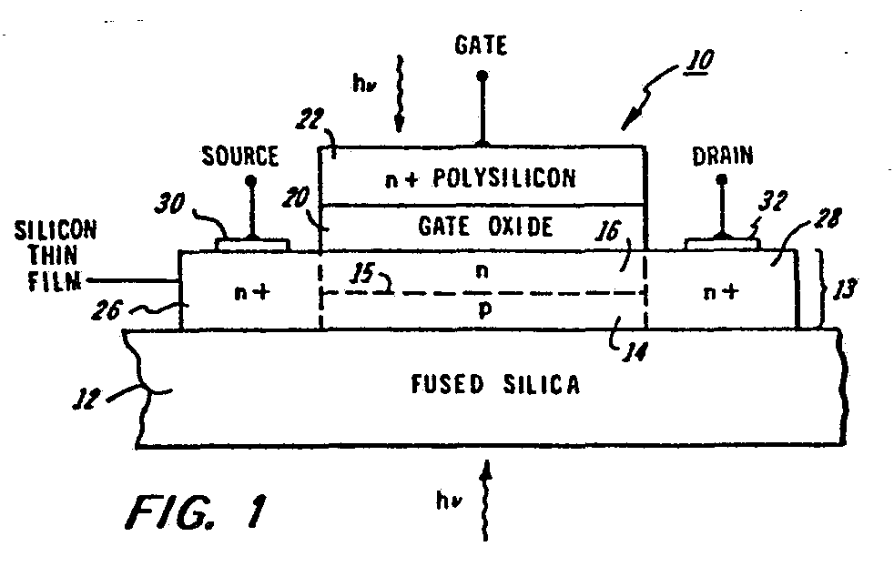
(57) A depletion mode thin film semiconductor photodetector (10) comprises a crystalline
silicon thin film (13) on an insulating substrate (12) with a source region (26),
a drain region (28) and a thin film light sensing channel region (14,16) formed therebetween.
A gate oxide (20) is formed over the channel region and a gate electrode (22) is formed
on the gate oxide. A p-n junction (15) is located parallel to the surface of the substrate
and within the thin film functioning as a space charge separation region in the channel.
The lower portion (14) of the channel region is a p region extending to the substrate
and the upper portion (16) of the channel region is a n region extending to the gate
oxide. The channel region functions as a fully depleted channel when the photodetector
is operated in its OFF state providing for high dynamic range and large photocurrent
operation. With n+ source and drain regions functioning as ohmic contacts to the channel n region the
device is a thin film transistor photodetector which has high photoconductive gain
at low light intensities when the n channel region is fully pinched off by an applied
gate voltage to the gate electrode which is sufficiently negative as compared to the
threshold voltage of the photodetector. When the drain region (28) is replaced by
a p+ region functioning as an ohmic contact to the channel p region, a depletion mode
gated diode is formed (see Figure 7). When the channel region is extended to include
a plurality of linearly spaced gate electrodes (22A, 22',228) formed on the gate oxide
region with an input diode (lD) formed adjacent to the first of such gate electrodes
(22A) and an output diode (OD) formed adjacent to the last of such gate electrodes
(228) the photodetector functions as a charge coupled device (see Figure 8).
|
|
