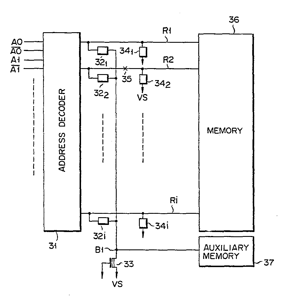
(57) A semiconductor memory device is disclosed in which, when a main memory (36) contains
an error bit cell, the main memory (36) is switched to an auxiliary memory (37) by
cutting off an interconnection wire between a decoder (31) and the main memory (36),
and subjecting a high resistance polysilicon (32,, 322, ...) connected between the decoder (31) and the auxiliary memory (37) to laser annealing
to reduce the resistance of the high resistance polysilicon (321, 322, ...) and to connect the decoder (31) and the auxiliary memory (37).
|
|
