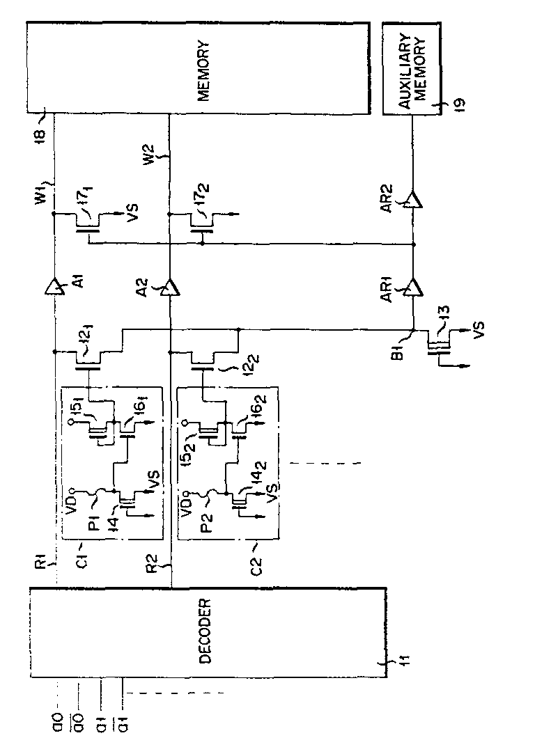
(57) A semiconductor memory device is disclosed, which comprises a main memory (18), a
decoder (11) for selecting the main memory (18), an auxiliary memory (19), transistors
(171 172, ...) connected between the auxiliary memory (19) and the decoder (11) for selecting
the auxiliary memory (19) according to the output of the decoder (11), and circuits
(C,, C2, ...) for controlling the transistors (121 122, ...). The transistors (12,, 122, ...) render the main memory (18) inoperative when the auxiliary memory (19) is rendered
operative.
|
|
