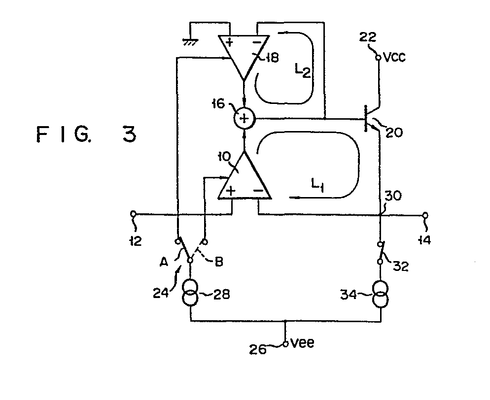
(57) (D A sampling circuit generally suitable for a sample-and-hold circuit is disclosed
which includes two differential amplifiers (10, 18) selectively rendered operative
during the sampling and nonsampling periods, respectively; an adder (16) for receiving
output signals from the differential amplifiers (10, 18), and a switching bipolar
transistor (20). One differential amplifier (10) is rendered operative during the
sampling period. The output signal from this differential amplifier (10) is negatively
fed-back through the adder (16) and the switching bipolar transistor (20) to the inverting
input terminal thereof connected to an output terminal (14) of the sampling circuit.
However, during the nonsampling interval, the other differential amplifier (18) is
rendered operative. The output signal from this differential amplifier (18) is fed
back to the inverting input terminal thereof through the adder (16). Therefore, the
switching bipolar transistor (20) is rendered nonconductive, and the analog signal
supplied to an input terminal (12) of the sampling circuit is prevented from being
transferred to the output terminal (14) of the sampling circuit.
|
|
