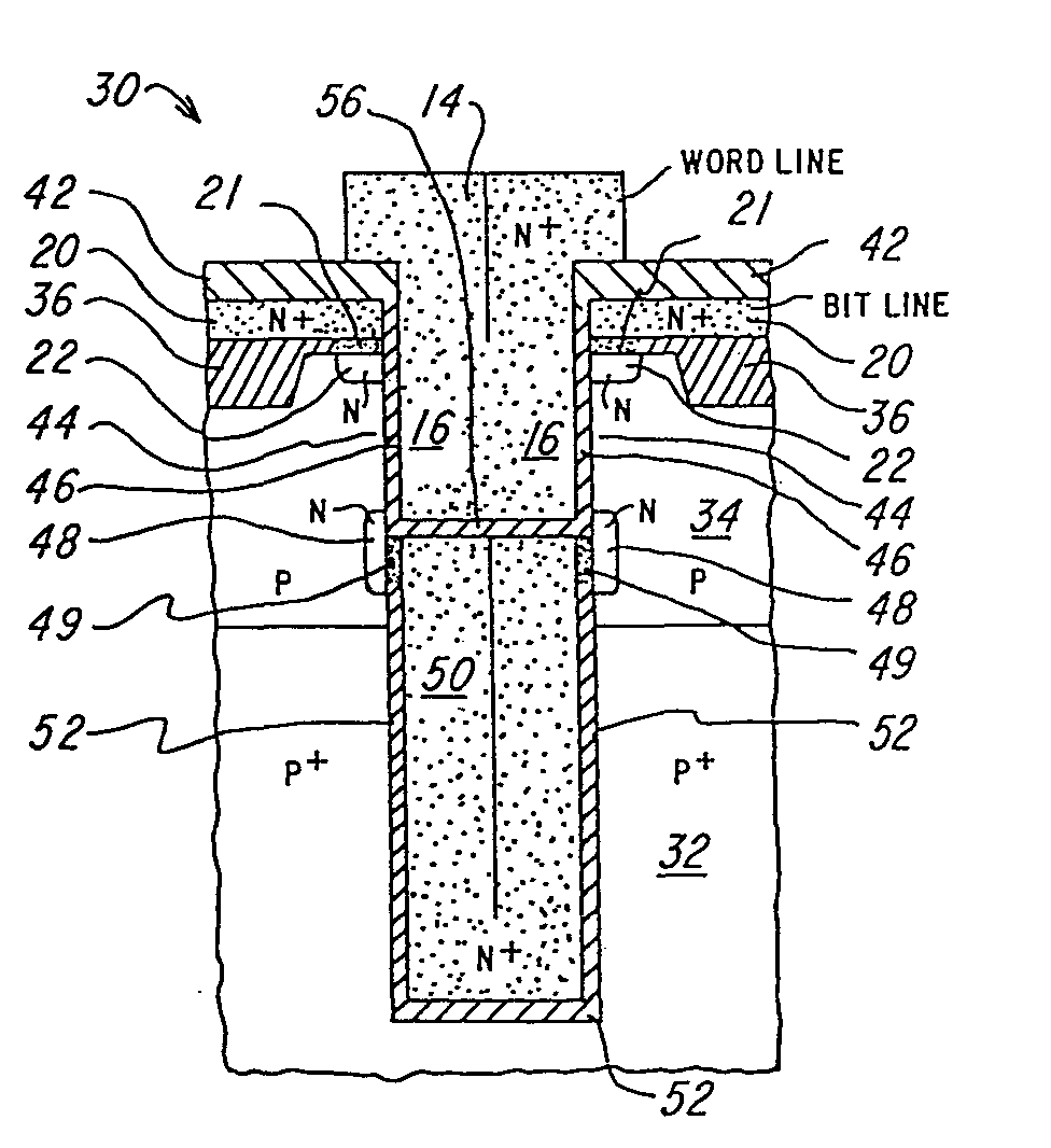
(57) A dRAM cell and array of cells, together with a method of fabrication, are disclosed
wherein the cell includes one field effect transistor and one storage capacitor with
both the transistor and the capacitor formed in a trench in a substrate. The transistor
source (22), channel (44) and drain (48) and one capacitor plate (32) are formed essentially
vertically in the bulk substrate sidewalls of the trench, and the gate (16) and other
capacitor plate (50) are formed in two regions of material inserted into the trench
and isolated from the bulk by an insulating layer (52, 46). Signal charge is stored
on the capacitor material inserted into the trench by an electrical connection of
the bulk substrate source to the capacitor material through the insulating layer.
In preferred embodiments word lines (14) on the substrate surface connect to the upper
of the inserted regions which forms the gate, and bit lines (20) on the substrate
surface form the drains. The trenches and cells are formed at the crossings of bit
lines and word lines; the bit lines and the word lines form perpendicular sets of
parallel lines.
|
|
