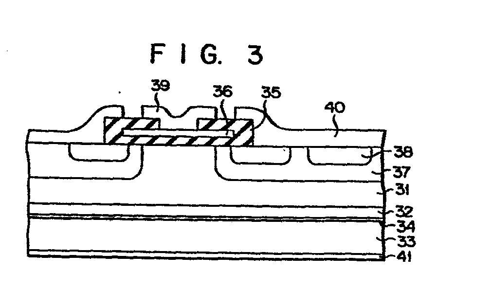
(57) A conductivity modulation type semiconductor device comprises a semiconductor anode
substrate (33) of a P type having two surfaces, a semiconductor substrate (31) of
an N type having two surfaces, the semiconductor substrate having a high impurity
layer-like region (32) on one surface thereof and a low concentration drain region
on the other surface thereof, a body region (37) of P type formed in the drain region
and exposed at one surface of the semiconductor substrate, source regions (38) of
an N type formed in the body region and exposed at the other surface of the semiconductor
substrate, and a gate layer (36) formed within the insulating layer, which extends
between the source and drain regions, on the body region. The other surface of the
anode substrate is polished and is intimately joined to the polished surface of the
semiconductor substrate to form a junction layer therebetween.
|
|
