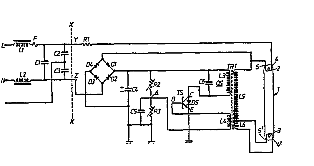
(57) An electronic ballast for a discharge lamp has a transistor-oscillator arrangement
comprising a single transistor (TS), whose base is coupled to be driven via a feedback
winding (L4) of a transformer (TR1). A primary winding (L3) of the transformer forms
part of a resonant circuit connected in the collector path of the transistor. A secondary
winding (L5) of the transformer is connected across a discharge lamp (1) for the supply
of high frequency alternating voltage to the lamp.
The transistor is biased into class A operation, by a biasing means (R2, R3). This
biasing means can also be used as a dimmer by adjusting the operation of the transistor
along its characteristic curve to alter the collector voltage.
The ballast has lamp connector terminals, 4, 5 a first one 4 ofthe terminals being
connected to an a.c. voltage supply (L), and the second of the connector terminals
(5) being connected to a rectifying means (D1-D4). This ensures that the ballast only
operates when an operative filament (2) is connected between the lamp connector terminal
(4, 5).
Mains supply voltage is filtered by a line filter L1, 12, C1-C3.
|
|
