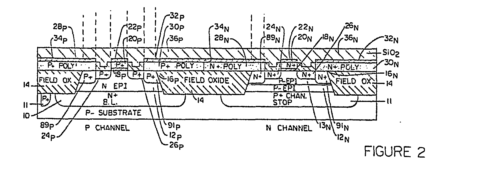
(57) There is disclosed a static RAM cell and MOS device for making the cell along with
a process for making the types of devices disclosed. The devices is an MOS device
built in an isolated island of epitaxial silicon similar to bipolar device Isolation
islands, and has single level polysilicon with self-aligned silicide coating for source,
drain and gate contacts such that no contact windows need be formed inside the isolation
island to make contact with the transistor. The static RAM cell formed using this
device uses extensions of the polysilicon contacts outside the isolation islands as
shared nodes to implement the conventional cross coupling of various gates to drain
and source electrodes of the outer transistors in the flip flop. Similarly, extensions
of various gate, source and drain contact electrodes are used as shared word lines,
and shared Vcc and ground contacts.
|
|
