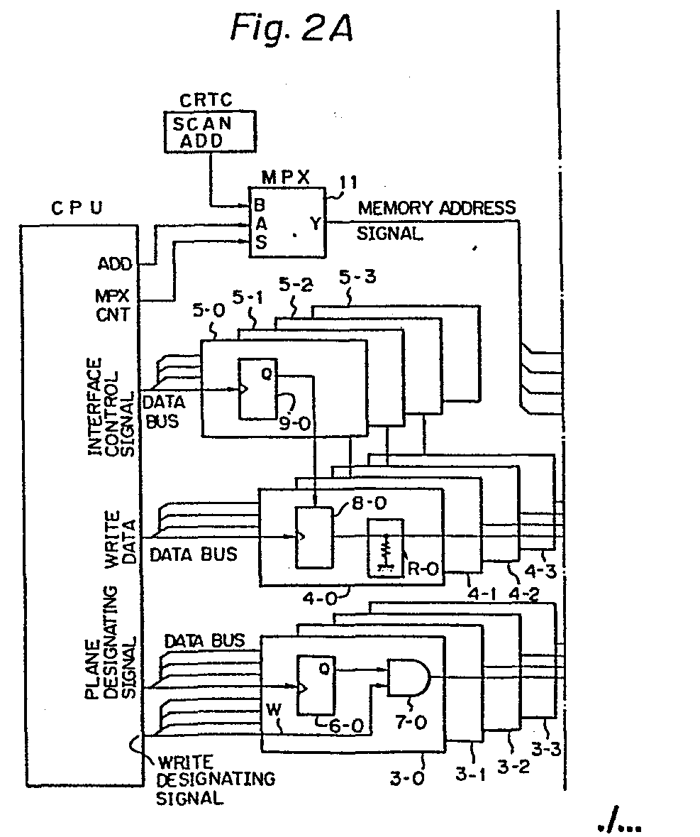
(57) A method for controlling memory planes in a writing operation in a display control
apparatus of a graphic system, the method including the steps of selectively connecting
a plurality of memory planes (2-0,...2-3) to a data bus (DATA BUS) by an interface
unit (4-0,...4-3f: selectively applying a write enable signal (WE) to the memory planes
from a plane designating unit (3-0,...3-31; applying data to be written to the data
bus from a central processing unit (CPU); writing the data into the memory planes
to which the write enable signal has been applied and which are connected to the data
bus; and writing predetermined fixed data into the memory planes to which is the write
enable signal has been applied but which are not connected to the data bus.
|
|
