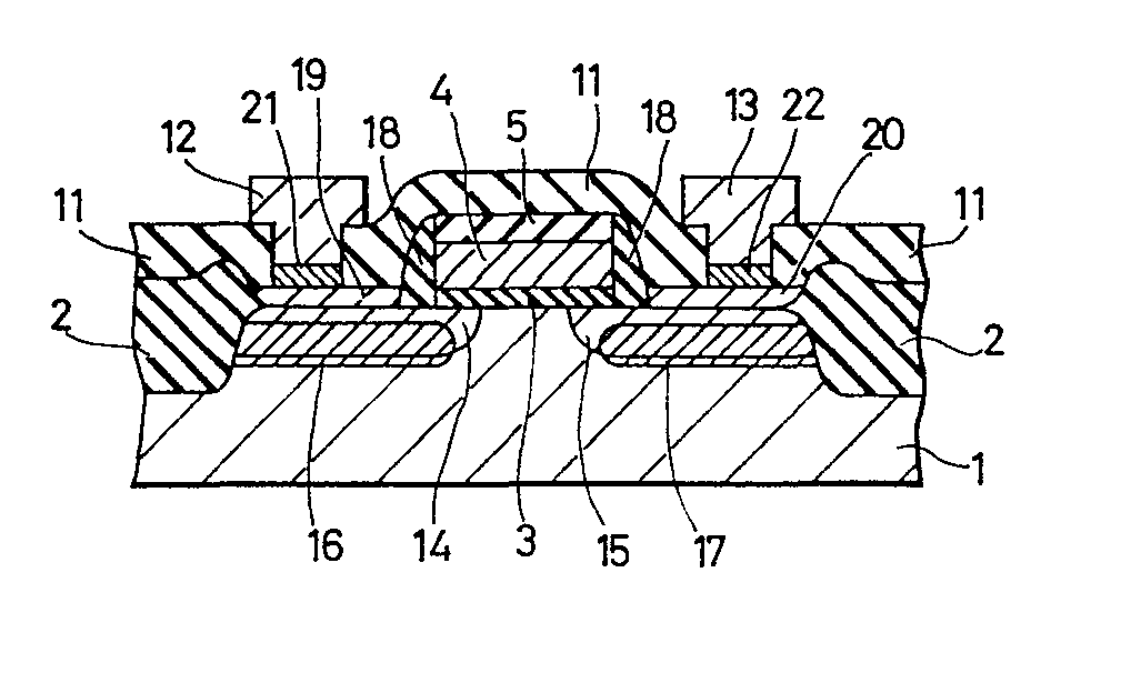
(57) In a field effect transistor, a drain region and a source region are constituted
by at least a first impurity distributed region (14, 15) and a second impurity distributed
region (16, 17). The first impurity distributed region (14,15) has a maximum impurity
concentration at the surface of a semiconductor substrate (1), the second impurity
distributed region (16, 17) has a maximum impurity concentration in the semiconductor
substrate (1), and at least the second impurity distributed region (16, 17) is formed
with a gate electrode edge as an impurity introduced window edge. The semiconductor
device has excellent breakdown voltage property, excellent current gain property,
and very stable and uniform characteristics.
|
|
