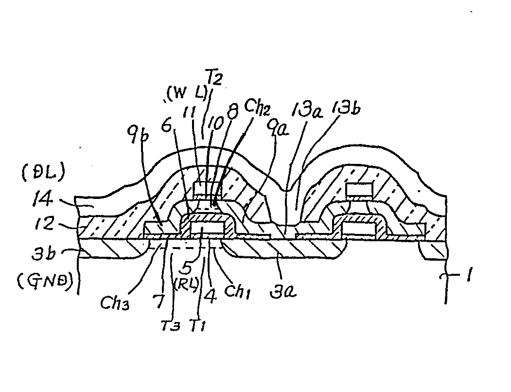
(57) 57 A three MIS transistor dynamic random access memory (DRAM) cell having a two-stored
structure, affording a high packing density, comprises a write select transistor (T2) disposed over a read select transistor (Ti). The transistors (Ti, T2) are separated from one another by an insulator layer (7), and a drain region of
the write select transistor (T2) is shared with the underlying read select transistor (Ti). A storage transistor (T3) and the read select transistor (Ti) are formed on a silicon substrate in the same level. Channel regions (Ch1, Ch3)
of the two transistors are connected to one another and each is used as a diffusion
(source or drain) region of the other of the two transistors.
A write select line (WL) and a read select line (RL) may be combined into a single
control line: a write/read select line (WRL), saving one line to obtain higher packing
density. In such a cell, gate electrodes of both read select and write select transistors
(T1, T2) are connected to the write/read line (WRL). These transistors are distinguished
from each other by having different threshold voltage levels from one another.
|
|
