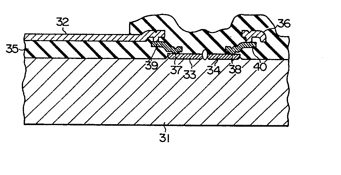
(57) For a protection of an integrated circuit fabricated on a semiconductor substrate
(31) of a first conductivity type against excess voltages applied thereto, there is
disclosed a protective device comprising a first impurity region (33) of a second
conductivity type formed in a surface portion of the semiconductor substrate and electrically
connected to a terminal plate (32) which supplies the integrated circuit with normal
external voltages, and a second impurity region (34) of the second conductivity type
formed in the surface portion of the semiconductor substrate and electrically connected
to a voltage supply layer (36) to which a difference voltage is applied, the second
impurity region being electrically insulated from the first impurity region under
the normal external voltages, a current path being established between the first and
second impurity regions under an application of an abnormal external voltages applied
through the terminal plate.
|
|
