(57) Transistors (10) having lateral gaps between their source and drain and the gate
are interconnected in a ROM to receive program code.
In one embodiment of the invention (Fig. 3), the gaps of selected transistors (42)
are subjected to a phosphorous implant (44) to create lightly doped n⁻ regions (26,28)
connecting the source (18) and drain (20) to the gate (14), and function normally.
The other transistors (40) do not receive the phosphorous implant, and thus have a
higher threshold voltage.
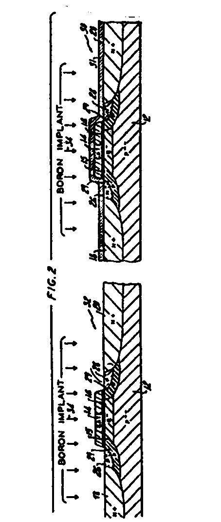
In another embodiment of the invention (Fig. 2) all of the transistors receive the
phosphorous implant to create the n⁻ regions (26,28) connecting the source and drain
to the gate, and the n- regions of selected transistors (32) are counter-doped with
a boron implant (34) so as to raise their threshold voltages, while the other transistors
(30) are not counter-doped and function normally.
In both embodiments, programming can occur late in the processing of the ROM.
|
|
