|
(11) | EP 0 151 418 B1 |

| (12) | EUROPEAN PATENT SPECIFICATION |
|
|
| (54) |
Pulse width modulation inverter system Wechselrichtersystem mit Pulsbreitenmodulation Système onduleur à modulation de largeur d'impulsion |
|
|
|||||||||||||||||||||||||||||||
| Note: Within nine months from the publication of the mention of the grant of the European patent, any person may give notice to the European Patent Office of opposition to the European patent granted. Notice of opposition shall be filed in a written reasoned statement. It shall not be deemed to have been filed until the opposition fee has been paid. (Art. 99(1) European Patent Convention). |
[0001] The present invention relates generally to a pulse width modulation (PWM) inverter system for converting a direct current (DC) power to an alternating current (AC) power. More particularly, the invention concerns an improvement of the pulse width modulation or PWM circuit.
[0002] The PWM DC-AC inverter is composed of a sinusoidal wave generating circuit for generating a sinusoidal wave corresponding to a fundamental wave of the output AC power and a triangular wave generating circuit for generating a triangular carrier, wherein the output wave form of both circuits are synthesized to prepare a string or row of pulses which constitutes a basic signal for a gate or base signal applied to switching elements constituting a major part of the inverter. However, in the inverter of the fixed circuit configuration mentioned above, a complicated peripheral circuit is required when the frequency of the fundamental wave or the carrier is to be altered, providing an obstacle to the inexpensive realization of the inverter system of a small size.
[0003] On the other hand, the capability of altering the frequency of the fundamental wave or carrier is an important factor not only for broadening the control range of loads powered by the inverter but also for avoiding mechanical and/or electrical vibrations. Additionally, it is desirable to increase the number of the output pulses relative to the fundamental wave in a low-frequency range of the inverter output power for the purpose of improving the waveform thereof, while decreasing the output pulse number or frequency in a high-frequency range of the inverter output to thereby improving the switching efficiency of the switching elements.
[0004] In GB-A-2107945 a PWM inverter system is disclosed for converting DC power to AC power comprising an output voltage setting circuit for generating a pattern of output voltage corresponding to a speed command value, an oscillator for generating a pulse train having a frequency proportional to said speed command value and a PWM signal producing circuit. This known system makes use of a ROM (read only memory) which provides in response to input pulses of a binary counter a programmed output for controlling a switch circuit which connects each power conductor leading to a motor with positive and negative DC, but this known system needs a great amount of previously prepared data and it is cumbersome to cope with changes in the operating conditions.
[0005] Under the circumstances, there is a tendency of replacing the conventional analogue control circuit by a digital control circuit, as is proposed in Japanese Patent Application Laid-Open Nos. 157.275/1981 and 43.573/1981, by way of example. However, the PCM systems proposed heretofore suffer shortcomings in that an expensive memory circuit of a large storage capacity is required for storing the switching pattern of the switching elements as a function of the output frequency, complicated arithmetic operation is required for deriving the gate (base) signal for the switching elements and so on, presenting thus difficulty in implementing inexpensively the inverter system of an improved controllability.
[0006] Accordingly, it is an object of the present invention to provide a pulse width modulation or PWM inverter system of an improved controllability.
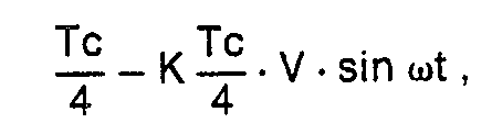
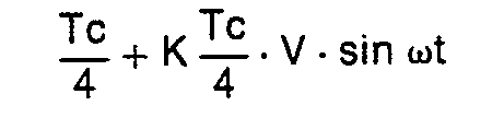
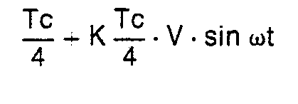
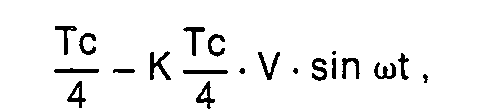
[0007] This object is achieved by the present invention by providing a PWM inverter system for converting DC power to AC power, comprising an output voltage setting circuit for generating a pattern of output voltage value corresponding to a speed command value ; an oscillator for generating a pulse train having a frequency proportional to said speed command ; and a PWM signal producing unit for applying PWM control signals to each of a pair of upper and lower arms constituting an inverter bridge, characterized in that said PWM signal producing unit is including : a frequency division circuit for dividing the frequency of said pulse train produced by said oscillator to produce interrupt pulses ; a pulse interval measuring circuit for measuring a pulse interval between predetermined ones of said interrupt pulses supplied from said frequency division circuit ; an arithmetic unit responding to the input of said interrupt pulses from said frequency division circuit to produce a timing signal corresponding to the timing at which said interrupt pulse is inputted and for updating the data associated with the current operating phase relative to a fundamental wave, and for performing arithmetic operations at every input of the interrupt pulse alternately in accordance with
[0008]
and
where V represents the output voltage value, Tc represents the pulse interval, wt represents the operation phase relative to the fundamental wave, and K represents a proportional constant, to thereby produce pulse width data corresponding to the result of the arithmetic operations ; a pulse width conversion circuit supplied with said pulse width data from said arithmetic unit for producing a width pulse train conforming to said pulse width data at every timing signal supplied from said arithmetic unit ; and a waveform processing circuit supplied with said width pulse train from said pulse width conversion circuit and said timing signal from said arithmetic unit to produce sequentially phase output pulse trains.
[0009] The present invention will be apparent from the following detailed description taken in conjunction with the accompanying drawings, in which :
Fig. 1 is a block diagram showing a general arrangement of a PWM DC-AC inverter system according to an exemplary embodiment of the present invention ;
Fig. 2 is a timing chart for illustrating operation of the system shown in Fig. 1 ; and
Fig. 3 is a flow chart for illustrating operation of the same system.
[0010] As the result of a series of studies and analysis of various inverter control circuits or systems, the inventors have found that various processing operations required for the inverter control can be reduced or mitigated by processing a string or train of pulse signals for controlling the switching elements of the inverter in accordance with the following expression :
where Tp represents the pulse width of the individual pulses constituting the phase output pulse train which provides the basis for the inverter control, K represents a proportional constant, Tc represents a time interval at which the pulses are produced, V represents the output voltage of the inverter, and wt represents the phase of the pulse signal relative to the fundamental wave.
[0011] In the following, an inverter system which is so implemented as to satisfy the condition given by the expression (1) will be described by referring to Fig. 1 which shows in a block diagram an arrangement of the inverter system embodying the invention. In Fig. 1, a reference numeral 1 denotes a converter for converting an AC power supplied from a three-phase AC power supply 2 to a DC power, 3 denotes a smoothing capacitor inserted in a DC circuit connected to the output of the AC-DC converter 1, and 4 an inverter bridge circuit for converting again DC power to a three-phase AC power. In the illustrated system, the switching elements are constituted by transistors. The major circuits of the inverter system mentioned above are controlled by a control circuit which will be described in detail hereinafter. In Fig. 1, a reference numeral 5 denotes a three-phase induction motor connected to the output of the inverter system, 6 denotes a resistor inserted in the DC circuit for detecting an overcurrent, and 7 denotes a wire or line for detecting an overvoltage in the DC circuit, both the resistor 6 and the line 7 being connected to the control circuit through an interface circuit 8 for supplying respective detection signals to the control circuit.
[0012] Now, description will be made in detail on the arrangement of the control circuit. In Fig. 1, a reference numeral 10 denotes a speed setting or command circuit for presetting the frequency of the output voltage of the inverter system and hence the operation or rotation speed of the three-phase induction motor 5. A numeral 11 denotes a ramp circuit for adjusting or regulating the time required for accelerating -or decelerating the three-phase induction motor 5 to the speed level preset by the speed command circuit 10 in conformance with the load characteristic of a load connected to the output shaft of the induction motor 5. A numeral 12 denotes an output voltage command circuit which responds to the speed command signal supplied through the ramp circuit 11 to produce signals representative of the output voltage patterns or profiles of the inverter system corresponding to the desired controls of the induction motor operation such as constant torque control operation, constant output control operation or the like. A numeral 13 denotes an oscillator for producing a pulse train of a pulse frequency proportional to the speed command value. A numeral 14 denotes a frequency division circuit for dividing the frequency of the pulse train produced by the oscillator 13 to thereby produce a pulse train indicative of the time interval at which the phase output pulses constituting the fundamental wave are produced. In other words, the relationship between the speed command value and the oscillation frequency of the oscillator 13 as well as the division ratio of the frequency division circuit 14 are previously so selected that the pulse train conforming to the time interval at which the phase output pulses make appearance can be produced. A numeral 15 denotes a pulse interval measuring or detecting circuit for measuring the interval at which a particular or predetermined pulse makes appearance in the pulse train produced by the frequency division circuit 14, the result of measurement being outputted as a pulse interval data signal. A numeral 16 denotes an analogue-to-digital or A/D converter for converting the analogue data of the output voltage command V and the speed command f into corresponding digital data. A numeral 17 denotes an arithmetic and logical processing unit (referred to simply as arithmetic unit) for executing predetermined arithmetic operations on various input data in accordance with program, both of which are previously stored in a memory 18. More specifically, the memory 18 stores therein program data and various table data required for the arithmetic operation executed by the arithmetic unit 17 and contains work areas saved for the operations of the arithmetic unit 17. A numeral 19 denotes a pulse width conversion circuit (also referred to as timer circuit) constituted by a sort of timer which responds to the command signals supplied from the arithmetic unit 17 for producing a width pulse train containing width pulse signals each representing the pulse width corresponding to the pulse width data resulting from the operation of the arithmetic unit 17. A numeral 20 denotes a waveform processing circuit composed of D-type flip-flops as the basic components. The waveform processing circuit 20 receives the data signal from the arithmetic processing unit 17 and the width pulse signal from the pulse width conversion circuit 19 as the clock inputs for producing sequentially the phase output pulses. A numeral 22 denotes a phase output distribution circuit and a numeral 21 denotes a signal amplifier. The phase output distribution circuit 22 serves to distribute the phase output pulses among the upper and lower arms for each phase of the three-phase inverter bridge circuit 4, whereby the phase output pulses amplified through the signal amplifier 21 are supplied as the base or gate drive signals to the individual switching elements constituting the inverter bridge circuit 4. Finally, a reference numeral 23 denotes an abnormality detecting circuit for detecting possible abnormalities of the three-phase power supply network 2 such as momentary service interruption, undervoltage condition or the like, the result of the detection being transmitted to the arithmetic unit 17 by way of the interface 8. Further, upon detection of the overcurrent and/or overvoltage in the DC circuit, the momentary service interruption of the three-phase power supply network and the undervoltage condition, the interface circuit 8 produces an emergency breaking signal to the phase output distribution circuit 21, which in turn responds to these abnormality signals to stop the distribution of the phase output pulses among the switching elements for assuring the protection of the inverter bridge circuit.
[0013] With the arrangement of the control circuit described above, operation thereof will be elucidated by referring to a timing chart shown in Fig. 2 and a flow chart shown in Fig. 3. When the phase output pulse train of the inverter is to be represented by pulse signals of positive potential or level and zero potential or level, the phase output pulse train will be in such a form of pulse signal train as illustrated at (b) in Fig. 2, in which duration of the positive potential or the zero potential varies progressively. In this conjunction, the relationship between the fundamental wave and the carrier employed heretofore in the inverter control will be considered. When the waveform of the fundamental wave is represented by S with that of the carrier being represented by M as shown in Fig. 2 at (a), the phase output pulse train is derived in the form of the pulse train shown at (b) from the relationship between the fundamental waveform S and the carrier waveform M. More specifically, the durations of the low and high potential levels Lo and Hi of the phase output pulse train (b) are substantially equal to each other in the vicinity of the zero-cross of the fundamental waveform S. On the other hand, in the positive range of the fundamental wave S, the duration of the low or zero potential Lo of the phase output pulse train (b) becomes shorter as the absolute value of the fundamental wave S increases. On the other hand, within the negative range of the fundamental wave S, the duration of the low or zero potential Lo of the phase output pulse train (b) becomes longer as the absolute amplitude of the fundamental wave S increases. Further, when the carrier M is additionally considered, it will be seen that, within a period Tc of the carrier M between the successive positive and negative peaks thereof, a time interval TP, between the positive peak of the carrier M and the succeeding time point at which the phase output pulse signal (b) rises to the positive or high level Hi becomes shorter as the absolute value of the fundamental wave S is increased in the positive range. On the contrary, a time interval TP2 between the negative peak of the carrier M and a succeeding time point at which the phase output pulse signal (b) changes to the zero level Lo becomes shorter as the absolute value of the fundamental wave S is increased in the negative range thereof. In other words, the intervals Tp1 and Tp2 under consideration can be expressed in terms of a quarter-period of the carrier M as follows :
[0014] In light of the result of the above analysis, the phase output pulse train or signal (b) is derived by correspondingly controlling the intervals TP, and TP2 in the case of the illustrated embodiment.
[0015] The control will be further described by referring to the flow chart shown in Fig. 3 in combination with the block diagram shown in Fig. 1. When the oscillator 13 starts oscillation in response to the speed command value, the frequency divider circuit 14 receives the pulse train outputted from the oscillator 13 to count the pulses and produces an interrupt pulse p (Fig. 2) every time the number of the counted pulse has attained the value corresponding to the frequency division ratio which is previously so determined in consideration of the inverter output frequency that twice as many as the pulses of the phase output pulse train (b) are available for constituting one cycle of the inverter output signal. Data of the frequency division ratios for the desired inverter output frequencies are previously stored in the memory 18. In this way, the interrupt pulse p is produced periodically at every positive and negative peak of the carrier M made use of in the prior art inverter control. The data of frequency division ratio stored in the memory 18 is supplied to the frequency division circuit 14 by way of the arithmetic unit 17. In the case of the illustrated embodiment, the pulse interval measuring circuit 15 is adapted to measure the pulse interval at every other pulse as the pulse interval between the successive particular or predetermined pulses mentioned hereinbefore.
[0016] In response to every interrupt signal p produced from the frequency division circuit 14, the arithmetic unit 17 executes an interrupt routine illustrated in Fig. 3 in accordance with the corresponding program stored in the memory 18. More specifically, upon activation of the interrupt routine, the arithmetic unit 17 firstly inverts the data signal shown in Fig. 2 at (c), which data signal is supplied to the waveform processing circuit 20. Subsequently, the arithmetic unit 17 produces a command signal for activating the timer circuit (or pulse width conversion circuit) 19 which operates on the basis of timing data for generating the phase output pulse train, the data having been arithmetically determined in the execution of the preceding interrupt routine. Next, the arithmetic unit 17 updates the current or instant phase data for the fundamental wave S located in the work area of the memory 18. This is because the phase interval to be updated at every interrupt pulse is determined as the number of the interrupt pulses for the fundamental wave S is determined on the basis of the phase output pulse number (or frequency of the carrier M employed heretofore) for every range of the predetermined speed command values (inverter output frequencies). More specifically, since a number of the interrupt pulses which are twice as many as the pulses constituting an output phase pulse train outputted during a single period of the fundamental wave S are generated at an equi-interval during the single period of the fundamental wave S, the current phase data for the fundamental wave S is updated in response to every interrupt pulse by a value corresponding to a quotient resulting from division of 2-ir by the number of interrupt pulses generated during the single period of the fundamental wave S. Next, the arithmetic unit 17 fetches the pulse interval data Tc from the pulse interval measuring circuit 15 and stores the data in the working area of the memory 18 for the succeeding arithmetic processing. Subsequently, the arithmetic unit 17 fetches the speed command input through the A/D converter 16 for comparison with the data representing the relation between the inverter output frequency and the frequency division ratio stored in the memory 18 in the form of a data table. When it is determined on the basis of the result of comparison that no necessity exists for changing the frequency dividing ratio, i. e. the number of the phase output pulses for one cycle of the fundamental wave, the routine proceeds to the next step where the output voltage value of the output voltage command circuit 12 is fetched by the arithmetic unit 17 through the A/D converter 16 to be stored in the working area of the memory 18 for the subsequent arithmetic processing. Subsequently, the arithmetic unit 17 makes reference to a sine table stored previously in the memory 18 and containing data concerning the relations between the phases of the phase output pulses and the instantaneous values at the operating phase position of the fundamental wave S, to read the data of the required instantaneous value (sin wt) on the basis of the updated operating phase data. The result of the reading operation is temporarily stored in a working area of the memory 18. Next, the arithmetic unit 17 arithmetically determines the timing for pulse generation in accordance with the expression (2) or (3) mentioned hereinbefore on the basis of the pulse interval data Tc, the output voltage value data V and the instantaneous value data sin wt fetched at the respective preceeding steps. At first, the pulse interval Tu for the V-phase is calculated. More specifically, when the data signal c inverted and held at the start of the interrupt routine is at the low or zero level Lo, the timing TU1 at which the phase output pulse b rises up is determined in accordance with the expression (2). Namely,
[0017] On the other hand, when the data signal c is at the high or positive level Hi, the timing TU2 at which the phase output pulse b falls is arithmetically determined in accordance with the expression (3). Namely,
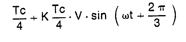
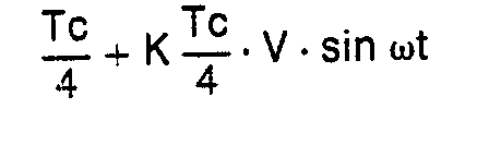
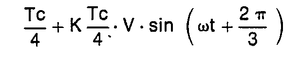
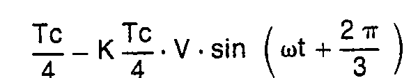
[0018] The expressions (4) and (5) are alternately selected in every execution of the interrupt routine, wherein the result of the arithmetic operation is transferred to a temporary storage area for the U-phase data saved in the timer circuit 19 at the succeeding step. After the transfer of the U-phase pulse timing data Tu has been completed, the arithmetic unit 17 reads from the sine table the instantaneous value of the fundamental wave S which differs by (2/3)ir in phase from the updated operating phase data, to thereby calculate the V-phase pulse timing Tv on the basis of the data read out from the sine table in accordance with
[0019] The calculated data of the timing Tv at which the V-phase output pulse rises up or falls is also transferred to a temporary storage area for the V-phase data reserved in the timer circuit 19 at the succeeding step. Finally, the timing at which the W-phase output pulse rises up or falls is determined on the basis of the timing data Tu and Tv for the U- and V-phases, respectively, in accordance with
[0020] The calculated W-phase timing data Tw is also transferred to the temporary storage area for the W-phase data reserved in the timer circuit (or pulse width conversion circuit) 19. Of course, the results of the timing calculation for the U-phase and V-phase pulses are stored also in the working area of the memory 18 for performing the calculation in accordance with the expression (7). In this manner, the arithmetic unit 17 executes the interrupt routine in response to each interrupt signal p supplied from the frequency division circuit 14, to thereby activate the timer circuit 19 on the basis of the calculated timing data Tu, Tv and Tw, while calculating the timing data for the following activation of the timer circuit 19.
[0021] Next, changing of the frequency dividing ratio as effected in the occurrence of executing the interrupt routine will be described. The arithmetic unit 17 fetches as the input thereto the speed command value and makes reference to the table which is stored in the memory 18 and contains the data of the inverter output frequencies and the frequency dividing ratios. When it is determined that the speed command value necessitating the changing of the frequency dividing ratio has been attained, the processing mentioned below is performed starting from the time point at which the phase of the fundamental wave S is 0°, i. e. the updated operating phase is 0°. At first, a new frequency dividing ratio is read out from the table containing the data of the inverter output frequencies and the frequency dividing ratios, and the data read out is transferred to the frequency divider circuit 14. Since the periodical time interval at which the interrupt pulse p is produced must naturally be altered, the periodical time interval at which every other interrupt pulse p is to be produced in correspondence to the new speed command is calculated on the basis of the data stored previously in the data table placed in the memory or the period of the fundamental wave S corresponding to the new speed command, the oscillation period of the oscillator 13, the frequency dividing ratio of the frequency divider circuit 14 and/or the like data, the result of the calculation being utilized for correcting the pulse interval data Tc stored in the working area of the memory 18. In succession to the changing of the frequency dividing ratio and the correction of the frequency dividing ratio and the correction of the pulse interval data, the interrupt routine described hereinbefore is regained to be executed.
[0022] Upon preparation of the timing data (Tul, Tu2, ..., TVa, ..., Tw3) concerning the rising and falling of the phase output pulses, the timer or pulse width conversion circuit 19 operates as the timer in response to the command signal outputted from the arithmetic processing unit 17 at every interrupt pulse input p. More specifically, so long as the circuit 19 performs the operation conforming to the pulse timing data in response to the command signal, the output of the timer circuit 19 is maintained at the level Lo which is restored to the level Hi upon completion of the timer operation. The signal waveform outputted from the timer circuit 19 at that time is illustrated in Fig. 2 at (d). Subsequently, the waveform processing circuit 20 receives the output signal d of the timer circuit as the clock signal input and performs the processing of the data signal c outputted from the arithmetic unit 17 on the basis of the clock signal d. More specifically, the waveform processing circuit 20 produces as the upper arm signal the signal representative of the level of the data signal c at the time point when the clock pulse d rises up and produces as the lower arm signal the signal c. Although the timer circuit 19 and the waveform processing circuit have been described in conjunction with only one phase, it goes without saying that the same signal processing is performed for three phases simultaneously. By operating the inverter by using the PWM signal prepared in the manner described above, the line current supplied to the three-phase induction motor is substantially of sinusoidal waveform.
[0023] According to the teaching of the invention, the PWM signal which has heretofore been obtained through synthesization of the fundamental wave and the carrier can be produced merely by repeating the relatively simple arithmetic operation. Further, since it is sufficient to store in the sine table only the instantaneous value data of the phase position at which the interrupt pulse is expected to make appearance, the amount of data required for the control can be significantly reduced. For practical application, it is sufficient to store previously the data in an amount which is less than the product of twice the number of the phase output pulses which constitute one cycle of the fundamental wave and the number of the varieties of the phase output pulses. Further, the amount of the data stored in the sine table can be reduced by a half by storing the data in an amount corresponding to a half period of the fundamental wave and exchanging the reading phase by the reading amount.
[0024] In the case of the embodiment described above, the system is constituted by hard logics in one part and by the arithmetic unit in the other part. However, when the arithmetic unit capable of processing at an adequately high speed is used, the PWM signal can be obtained only throught the arithmetic processing. In this connection, it should be noted that the time interval Tc at which the phase output pulses are produced is determined by the inverter output frequency FouT which in turn is determined by the speed command and the number PN of the pulses constituting one cycle of the fundamental wave in accordance with
Further the commanded inverter output voltage V can be expressed as follows :
where a and b are constants, respectively, and f represents the commanded speed. From the expressions (8) and (9), the expression (1) can be rewritten as follows :
[0025] Accordingly, the PWM signal can be produced through the arithmetic operation based on the expression (10) provided that it can be executed at a high speed.
[0026] Ideally, the pulse width of the phase output pulses is expressed by an integral of the pulses over the period of occurrence. Namely,
[0028] Accordingly, if the arithmetic operation in accordance with the above expression is possible, the pulse width modulation can be realized more ideally.
[0029] In the foregoing description, it has been assumed that the fundamental wave is of a sinusoidal waveform. However, it is possible to use a trapezoidal wave, a stepped wave or other waveform with a view to improving the waveform and reducing the memory capacity.
[0030] Although the output voltage command circuit is constituted by a sort of the function generator in the case of the illustrated embodiment, it is possible to store the voltage commands in a memory in the form of table together with the output frequency commands. Further, the output voltage data produced by the function generator can be partially corrected so that the voltage data may have more ideal value. To this end, data required for the correction may be stored in the memory.
[0031] The foregoing description has been made in detail in conjunction with the so-called synchronous inverter system in which the period of the fundamental wave coincides with that of the carrier. However, the invention is not restricted to such synchronous inverter system, but can be equally applied to the so-called asynchronous type inverter system. In the latter case, however, the amount of data to be stored in the sine table will be increased because the phase position at which the interrupt signal is produced varies relative to the fundamental wave. The increasing in the data amount may be obviated by adopting appropriate data reading procedure. It
[0032] In the case of the illustrated embodiment, the feed-back of the output frequency, the actual motor revolution number or the oscillation frequency of the oscillator is not adopted. However, it will be readily understood that the control operation can be effected on the basis of the data corrected appropriately through the feed-back of these parameters.
[0033] Further, in the case of the illustrated embodiment, data of the frequency dividing ratio and the pulse interval are updated only when the operating phase position relative to the fundamental wave is updated in response to the interrupt signal input which is produced when the inverter output attains the commanded value (output frequency). However, such data updating may be effected at the time when the operating phase is updated to 180°. In the case of the inverter system designed to producing the three-phase AC power, the data should preferably be updated at the time when any one of the three fundamental waves constituting the three phases, respectively, has attained 180° starting from 0°, i. e. when the operating phase position relative to the fundamental wave has attained the phase position given by a integral multiple of 60° starting from 0°. By effecting the data updating at such operating phase positions, the structure of data to be updated can be simplified.
[0034] Finally, it should be mentioned that the load monitoring processing for dealing with various abnormalities and protecting procedure may take place by making use of the residual time in the interrupt processing routine, although detailed description of these processings has been omitted because they constitute no parts of the invention.
[0035] As will be appreciated from the foregoing description, there has been provided according to the invention the PWM DC-AC inverter system which includes a PWM circuit which is capable of producing the phase output pulse having a pulse width corresponding to a product of a value associated with the inverter output voltage, a value associated with the inverter output pulse interval and the instantaneous value of the fundamental wave at the output phase position of the phase output pulse. The inverter system thus enjoys significantly improved controllability.
1. A PWM inverter system for converting DC power to AC power, comprising an output
voltage setting circuit (12) for generating a pattern of output voltage value corresponding
to a speed command value ; an oscillator (13) for generating a pulse train having
a frequency proportional to said speed command ; and a PWM signal producing unit for
applying PWM control signals to each of a pair of upper and lower arms constituting
an inverter bridge (4), characterized in that said PWM signal producing unit includes
: a frequency division circuit (14) for dividing the frequency of said pulse train
produced by said oscillator to produce interrupt pulses (Fig. 2p) ; a pulse interval
measuring circuit (15) for measuring a pulse interval between predetermined ones of
said interrupt pulses supplied from said frequency division circuit (14) ; an arithmetic
unit (17) responding to the input of said interrupt pulses from said frequency division
circuit (14) to produce a timing signal (Fig. 2c) corresponding to the timing at which
said interrupt pulse is inputted and for updating the data associated with the current
operating phase relative to a fundamental wave, and for performing arithmetic operations
at every input of the interrupt pulse (Fig, 2p) alternately in accordance with
and
where V represents the output voltage value, Tc represents the pulse interval, wt represents the operation phase relative to the fundamental wave, and K represents a proportional constant, to thereby produce pulse width data corresponding to the result of the arithmetic operations ; a pulse width conversion circuit (19) supplied with said pulse width data from said arithmetic unit (17) for producing a width pulse train (Fig. 2d) conforming to said pulse width data at every timing signal (Fig. 2c) supplied from said arithmetic unit (17) ; and a waveform processing circuit (20) supplied with said width pulse train (Fig. 2d) from said pulse width conversion circuit (19) and said timing signal (Fig. 2c) from said arithmetic unit (17) to produce sequentially phase output pulse trains (Fig. 2b).
2. A PWM inverter system according to claim 1, wherein said arithmetic unit (17) responds
to every input of the interrupt pulse (Fig. 2p) for outputting a command signal and
a timing signal constituted by a value inverting data signal, said pulse width converting
circuit (19) responds to the command signal from said arithmetic unit (17) for outputting
the width pulse train (Fig. 2d) conforming to the pulse width data supplied from said
arithmetic unit, and said waveform processing circuit (20) is supplied with the width
pulse train from said pulse width conversion circuit (19) and the data signal from
said arithmetic unit (17) for producing sequentially the phase output pulse trains
(Fig. 2b).
3. A PWM inverter system according to claim 2, wherein said pulse width conversion
circuit (19) responds to the command signal supplied from said arithmetic unit (17)
for inverting the output signal during a period corresponding to the pulse width data
supplied from said arithmetic unit.
4. A PWM inverter system according to claim 3, wherein said pulse width conversion
circuit (19) responds to the command signal supplied from said arithmetic unit (17)
for maintaining the output signal at a state Lo during a period corresponding to the
pulse width data supplied from said arithmetic unit.
5. A PWM inverter system according to claim 1, wherein said waveform processing circuit
(20) produces sequentially inverted phase output pulses upon every completion of the
inputting of the width pulse of said width pulse train (Fig. 2d) outputted from said
pulse width conversion circuit (19) during a period corresponding to the pulse width
data.
6. A PWM inverter system. according to claim 4, wherein said waveform processing circuit
(20) produces sequentially the phase output pulse trains (Fig. 2b) maintaining the
state of the data signal supplied from said arithmetic unit (17), when the width pulse
train (Fig. 2d) signal supplied from said pulse width conversion circuit (19) rises
up.
7. A PWM inverter system according to claim 1, wherein said arithmetic unit (17) responds
to the input of said interrupt pulses (Fig. 2p) from said frequency division circuit
(14) to update the data associated with the frequency dividing ratio corresponding
to said speed command value and the pulse interval.
8. A PWM inverter system according to claim 7, wherein said arithmetic unit (17) updates
the data concerning the frequency dividing ratio and the pulse interval when a predetermined
speed command value has been attained.
9. A PWM inverter system according to claim 8, wherein said arithmetic unit (17) updates
the data concerning the frequency division ratio and the pulse interval when a predetermined
speed command value has been attained and when the operation phase relative to the
fundamental wave has reached 0°.
10. A PWM inverter system according to claim 8, wherein a plurality of the speed command
values for updating the data of the frequency dividing ratio and the pulse interval
are previously prepared.
11. A PWM inverter system according to claim 10, wherein said arithmetic unit (17)
updates the data concerning the frequency dividing ratio and the pulse interval, when
a given one of said plural preset speed command values has been attained and when
the operating phase relative to the fundamental wave has attained a phase position
determined by an integral multiple of 60° starting from 0°.
12. A PWM inverter system according to claim 11, for obtaining a three-phase power,
said arithmetic unit (17) performs arithmetic processings upon every input of said
interrupt pulse alternately in accordance with

and

for a first phase, and in accordance with

for a second phase, where V represents the output voltage value, Tc represents the pulse interval, wt represents the operating phase relative to the fundamental wave, and K represents a proportional constant.
and
for a first phase, and in accordance with
for a second phase, where V represents the output voltage value, Tc represents the pulse interval, wt represents the operating phase relative to the fundamental wave, and K represents a proportional constant.
1. Wechselrichtersystem mit Pulsbreitenmodulation zum Umformen von Gleichstrom in
Wechselstrom, umfassend einen Ausgangsspannungsstellkreis (12), der einen Ausgangsspannungswertverlauf
entsprechend einer Drehzahlführungsgröße erzeugt ; einen Oszillator (13), der einen
Impulszug mit einer der Drehzahlführungsgröße proportionalen Frequenz erzeugt ; und
eine Pulsbreitenmodulationssignal-Erzeugungseinheit, die Pulsbreitenmodulations-Steuersignale
jeweils an einen oberen und einen unteren Zweig, die eine Wechselrichterbrücke (4)
bilden, anlegt, dadurch gekennzeichnet, daß die Pulsbreitenmodulationssignal-Erzeugungseinheit
aufweist: einen Frequenzteilerkreis (14), der die Frequenz des vom Oszillator erzeugten
Impulszugs unter Erzeugung von Unterbrechungsimpulsen (Fig. 2p) teilt ; einen Impulsintervallmeßkreis
(15), der ein Impulsintervall zwischen vorbestimmten Unterbrechungsimpulsen, die vom
Frequenzteilerkreis (14) zugeführt werden, mißt ; eine Recheneinheit (17), die aufgrund
der Eingabe der Unterbrechungsimpulse vom Frequenzteilerkreis (14) ein Taktsignal
(Fig. 2c) erzeugt, das dem Takt entspricht, mit dem der Unterbrechungsimpuls eingegeben
wird, und die der momentanen Arbeitsphase relativ zu einer Grundschwingung zugeordnete
Information aktualisiert und bei jeder Eingabe des Unterbrechungsimpulses (Fig. 2p)
Rechenoperationen abwechselnd nacheinander durchführt entsprechend

und
wobei V den Ausgangsspannungswert, Tc das Impulsintervall, αt die Arbeitsphase relativ zu der Grundschwingung und K eine Proportionalitätskonstante ist, um dadurch Pulsbreiteninformation entsprechend dem Ergebnis der Rechenoperationen zu erzeugen ; einen Pulsbreitenumformungskreis (19), dem die Pulsbreiteninformation von der Recheneinheit (17) zugeführt wird zur Erzeugung eines Breitenimpulszugs (Fig. 2d), der der Pulsbreiteninformation bei jedem von der Recheneinheit (17) zugeführten Taktsignal (Fig. 2c) entspricht; und einen Wellenformverarbeitungskreis (20), dem der Breitenimpulszug (Fig. 2d) von dem Pulsbreitenumformungskreis (19) und das Taktsignal (Fig. 2c) von der Recheneinheit (17) zugeführt wird zur sequentiellen Bildung von Phasenausgangsimpulszügen (Fig. 2b).
2. Wechselrichtersystem mit Pulsbreitenmodulation nach Anspruch 1, wobei die Recheneinheit
(17) auf jede Eingabe des Unterbrechungsimpulses (Fig. 2p) anspricht und ein Befehlssignal
sowie ein Taktsignal, das durch ein Wertumkehrungs-Datensignal gebildet ist, ausgibt,
wobei der Pulsbreitenumformungskreis (19) aufgrund des Befehlssignals von der Recheneinheit
(17) den Breitenimpulszug (Fig. 2d) entsprechend der von der Recheneinheit zugeführten
Pulsbreiteninformation ausgibt, und wobei dem Wellenformverarbeitungskreis (20) der
Breitenimpulszug von dem Pulsbreitenumformungskreis (19) und das Datensignal von der
Recheneinheit (17) zugeführt wird zur sequentiellen Bildung der Phasenausgangsimpulszüge
(Fig. 2b).
3. Wechselrichtersystem mit Pulsbreitenmodulation nach Anspruch 2, wobei der Pulsbreitenumformungskreis
(19) aufgrund des von der Recheneinheit (17) zugeführten Befehlssignals das Ausgangssignal
während einer Periode umkehrt, die der von der Recheneinheit zugeführten Pulsbreiteninformation
entspricht.
4. Wechselrichtersystem mit Pulsbreitenmodulation nach Anspruch 3, wobei der Pulsbreitenumformungskreis
(19) aufgrund des von der Recheneinheit (17) zugeführten Befehlssignals das Ausgangssignal
während einer Periode, die der von der Recheneinheit zugeführten Pulsbreiteninformation
entspricht, in einem Zustand Lo hält.
5. Wechselrichtersystem mit Pulsbreitenmodulation nach Anspruch 4, wobei der Wellenformverarbeitungskreis
(20) sequentiell phaseninvertierte Ausgangsimpulse bei jeder Beendigung der Eingabe
des Breitenimpulses des von dem Pulsbreitenumformungskreises (19) ausgegebenen Breitenimpulszugs
(Fig. 2d) während einer der Pulsbreiteninformation entsprechenden Periode erzeugt.
6. Wechselrichtersystem mit Pulsbreitenmodulation nach Anspruch 4, wobei der Wellenformverarbeitungskreis
(20) sequentiell die Phasenausgangsimpulszüge (Fig. 2b) erzeugt, die den Zustand des
von der Recheneinheit (17) zugeführten Datensignals aufrechterhalten, wenn das von
dem Pulsbreitenumformungskreis (19) zugeführte Breitenimpulszugsignal (Fig. 2d) ansteigt.
7. Wechselrichtersystem mit Pulsbreitenmodulation nach Anspruch 1, wobei die Recheneinheit
(17) aufgrund der Eingabe der Unterbrechungsimpulse (Fig. 2p) von dem Frequenzteilerkreis
(14) die dem Frequenzteilungsverhältnis zugeordneten Daten entsprechend dem Drehzahlführungswert
und das Impulsintervall aktualisiert.
8. Wechselrichtersystem mit Pulsbreitenmodulation nach Anspruch 7, wobei die Recheneinheit
(17) die das Frequenzteilungsverhältnis und das Impulsintervall betreffenden Daten
aktualisiert, wenn ein vorbestimmter Drehzahlführungswert erreicht ist.
9. Wechselrichtersystem mit Pulsbreitenmodulation nach Anspruch 8, wobei die Recheneinheit
(17) die das Frequenzteilungsverhältnis und das Impulsintervall betreffenden Daten
aktualisiert, wenn ein vorbestimmter Drehzahlführungswert erreicht ist und die Arbeitsphase
relativ zur Grundschwingung 0° erreicht hat.
10. Wechselrichtersystem mit Pulsbreitenmodulation nach Anspruch 8, wobei eine Mehrzahl
der Drehzahlführungswerte zur Aktualisierung der das Frequenzteilungsverhältnis und
das Impulsintervall betreffenden Daten vorher bereitgestellt wird.
11. Wechselrichtersystem mit Pulsbreitenmodulation nach Anspruch 10, wobei die Recheneinheit
(17) die das Frequenzteilungsverhältnis und das Impulsintervall betreffenden Daten
aktualisiert, wenn ein bestimmter der Mehrzahl vorgegebener Drehzahlführungswerte
erreicht ist und wenn die Arbeitsphase relativ zur Grundschwingung eine Phasenlage
erreicht hat, die durch ein ganzzahliges Vielfaches von 60°, ausgehend von 0°, bestimmt
ist.
12. Wechselrichtersystem mit Pulsbreitenmodulation nach Anspruch 11 zum Erhalt von
Drehstrom, wobei die Recheneinheit (17) bei jeder Eingabe des Unterbrechungsimpulses
abwechselnd nacheinander Rechenvorgänge entsprechend

und

für eine erste Phase und entsprechend

und
für eine zweite Phase durchführt, wobei V der Ausgangsspannungswert. Tc das lmpulsintervall, Mt die Arbeitsphase relativ zur Grundschwingung und K eine Proportionalitätskonstante ist.
und
für eine erste Phase und entsprechend
und
für eine zweite Phase durchführt, wobei V der Ausgangsspannungswert. Tc das lmpulsintervall, Mt die Arbeitsphase relativ zur Grundschwingung und K eine Proportionalitätskonstante ist.
1. Système onduleur MID pour la conversion d'une énergie à courant continu en une
énergie à courant alternatif, comprenant un circuit (12) de réglage de la tension
de sortie, servant à produire un profil de la valeur de la tension de sortie correspondant
à une valeur de commande de la vitesse ; un oscillateur (13) servant à produire un
train d'impulsions possédant une fréquence proportionnelle à ladite commande de la
vitesse : et une unité de production de signaux MID, servant à appliquer des signaux
de commande MID à chaque bras d'un couple de bras supérieur et inférieur constituant
un pont onduleur (4), caractérisé en ce que ladite unité de production de signaux
MID comporte : un circuit diviseur de fréquence (14) servant à diviser la fréquence
dudit train d'impulsions produit par ledit oscillateur de manière à produire des impulsions
d'interruption (figure 2p) ; un circuit (15) de mesure d'intervalles entre impulsions,
servant à mesurer un intervalle entre des impulsions prédéterminées faisant partie
desdites impulsions d'interruption délivrées par ledit circuit diviseur de fréquence
(14) : une unité arithmétique (17) répondant à l'arrivée desdites impulsions d'interruption
délivrées par ledit circuit diviseur de fréquence (14) de manière à produire un signal
de cadencement (figure 2c) correspondant au cadencement avec lequel ladite impulsion
d'interruption est introduite et servant à mettre à jour les données associées à la
phase actuelle de fonctionnement par rapport à une onde fondamentale, et à exécuter
alternativement des opérations arithmétiques lors de chaque arrivée de l'impulsion
d'interruption (figure 2p) conformément à

et
où V désigne la valeur de la tension de sortie. Tc désigne l'intervalle entre impulsions, wt désigne la phase de fonctionnement par rapport à l'onde fondamentale et K désigne une constante proportionnelle, de manière à produire des données de durées d'impulsions correspondant au résultat des opérations arithmétiques ; un circuit (19) de conversion des durées d'impulsions, alimenté par lesdites données de durées d'impulsions délivrées par ladite unité arithmétique (17) pour produire un train d'impulsions de durées (figure 2d) correspondant auxdites données de durées d'impulsions pour chaque signal de cadencement (figure 2c) délivré par ladite unité arithmétique (17) ; et un circuit (20) de traitement de formes d'ondes, recevant ledit train d'impulsions de durées (figure 2d) en provenance dudit circuit (19) de conversion des durées d'impulsions et ledit signal de cadencement (figure 2c) délivré par ladite unité arithmétique (17) de manière à produire successivement des trains d'impulsions de sortie de phase (figure 2b).
2. Système onduleur MID selon la revendication 1, dans lequel ladite unité arithmétique
(17) répond à chaque arrivée de l'impulsion d'interruption (figure 2p) pour délivrer
un signal de commande et un signal de cadencement constitué par un signal de donnée
d'inversion de la valeur, ledit circuit (19) de conversion des durées d'impulsions
répond au signal de commande délivré par ladite unité arithmétique (17) pour délivrer
le train d'impulsions de durées (figure 2d) correspondant aux données de durées d'impulsions
délivrées par ladite unité arithmétique, et ledit circuit (20) de traitement des formes
d'ondes est alimenté par le train d'impulsions de durées délivré par ledit circuit
(19) de conversion des durées d'impulsions et le signal de donnée délivré par ladite
unité arithmétique (17) pour produire successivement les trains d'impulsions de sortie
de phase (figure 2b).
3. Système onduleur MID selon la revendication 2, dans lequel ledit circuit (19) de
conversion des durées d'impulsions répond au signal de commande délivré par ladite
unité arithmétique (17) en inversant le signal de commande pendant une période correspondant
à la donnée de durée d'impulsion délivrée par ladite unité arithmétique.
4. Système onduleur MID selon la revendication 3, dans lequel ledit circuit (19) de
conversion des durées d'impulsions répond au signal de commande délivré par ladite
unité arithmétique (17) pour maintenir le signal de sortie dans un état Lo pendant
une période correspondant à la donnée de durée d'impulsion délivrée par ladite unité
arithmétique.
5. Système onduleur MID selon la revendication 4, dans lequel ledit circuit (20) de
traitement des formes d'ondes produit des impulsions de sortie de phase inversées
séquentiellement, lors de chaque achèvement de l'introduction de l'impulsion de durée
dudit train d'impulsions de durées (figure 2d), délivrée par ledit circuit (19) de
conversion des durées d'impulsions, pendant une période correspondant à la donnée
de durée d'impulsion.
6. Système onduleur MID selon la revendication 4, dans lequel ledit circuit (20) de
traitement des formes d'ondes produit successivement les trains d'impulsions de sortie
de phase (figure 2b) maintenant l'état du signal de donnée envoyé par ladite unité
arithmétique (17), lorsque le signal du train d'impulsions de durées (figure 2d),
envoyé par ledit circuit (19) de conversion des durées d'impulsions augmente.
7. Système onduleur MID selon la revendication 1, dans lequel ladite unité arithmétique
(17) répond à l'arrivée desdites impulsions d'interruption (figure 2p) délivrées par
ledit circuit diviseur de fréquence (14) pour mettre à jour les données associées
au rapport de division de fréquence correspondant à ladite valeur de commande de la
vitesse et audit intervalle entre impulsions.
8. Système onduleur MID selon la revendication 7, dans lequel ladite unité arithmétique
(17) met à jour les données relatives au rapport de division de fréquence et à l'intervalle
entre impulsions lorsqu'une valeur prédéterminée de commande de la vitesse a été atteinte.
9. Système onduleur MID selon la revendication 8, dans lequel ladite unité arithmétique
(17) .met à jour les données concernant le rapport de division de fréquence et l'intervalle
entre impulsions lorsqu'une valeur prédéterminée de commande de la vitesse a été atteinte
et que la phase de fonctionnement relative à l'onde fondamentale a atteint 0°.
10. Système onduleur MID selon la revendication 8, dans lequel une pluralité des valeurs
de commande de la vitesse pour la mise à jour des données du rapport de division de
fréquence et de l'intervalle entre impulsions sont préalablement préparés.
11. Système onduleur MID selon la revendication 10, dans lequel ladite unité arithmétique
(17) met à jour les données concernant le rapport de division de fréquence et l'intervalle
entre impulsions, lorsqu'une valeur donnée faisant partie de ladite pluralité de valeurs
préréglées de commande de la vitesse a été atteinte et que la phase de fonctionnement
par rapport à l'onde fondamentale a atteint une position de phase déterminée par un
multiple entier de 60° à partir de 0°.
12. Système onduleur MID selon la revendication 11, pour l'obtention d'une énergie
triphasée, dans laquelle ladite unité arithmétique (17) exécute alternativement des
traitements arithmétiques lors de chaque arrivée de ladite impulsion d'interruption,
conformément à :
et
pour une première phase, et conformément à
t

pour une seconde phase, V désignant la valeur de la tension de sortie, Tc l'intervalle entre impulsions, ωt la phase de fonctionnement relative à l'onde fondamentale et K une constante proportionnelle.
et
pour une première phase, et conformément à
t
pour une seconde phase, V désignant la valeur de la tension de sortie, Tc l'intervalle entre impulsions, ωt la phase de fonctionnement relative à l'onde fondamentale et K une constante proportionnelle.