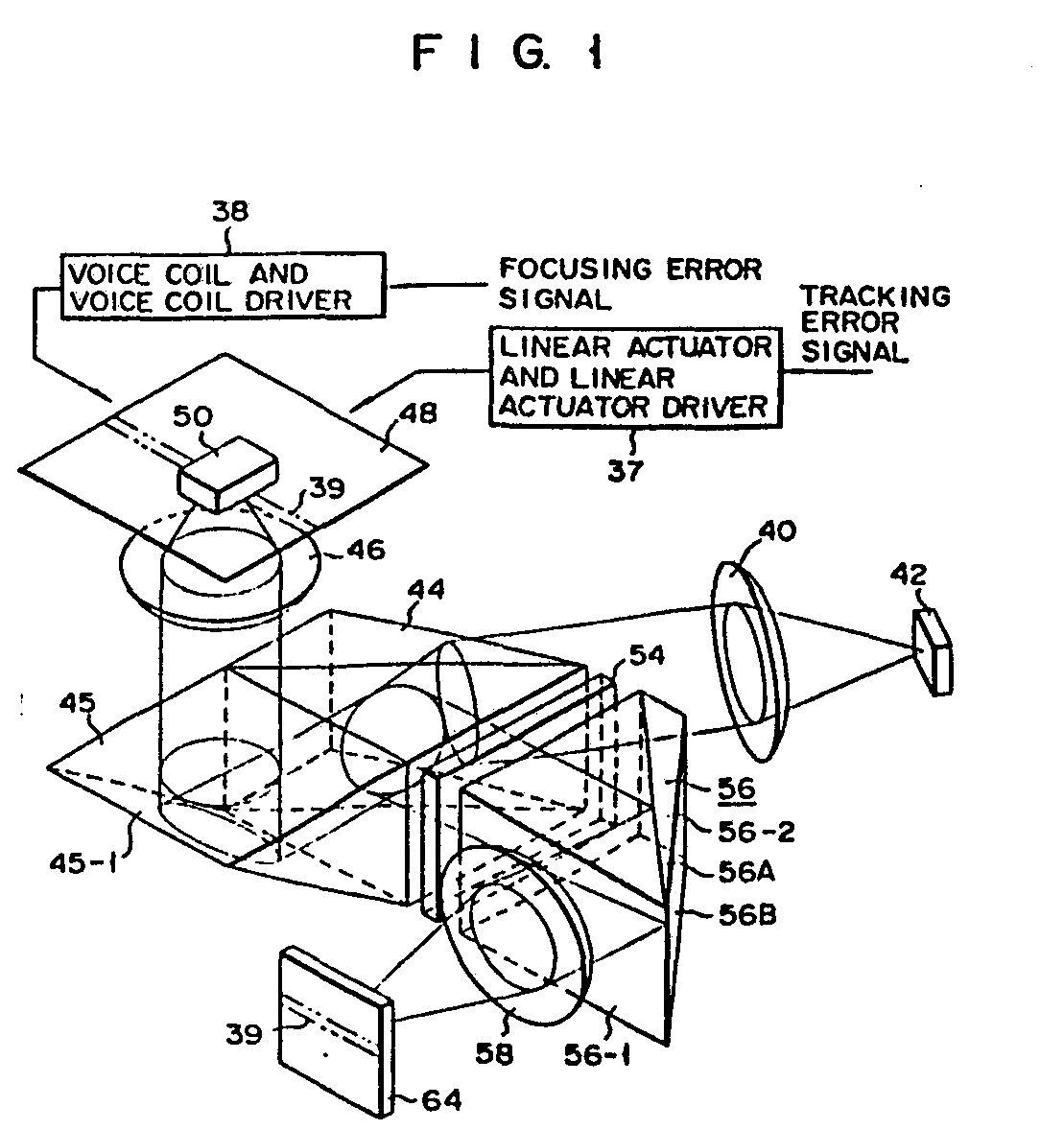
(57) An optical system for use with an optical memory (48) including an optical arrangement
(56) for separating light reflected from the surface of the optical memory (48) into
a plurality of different resultant beams. This optical mechanism (56) comprising four
reflecting surfaces (56A, 56B-1, 568-2, 56B-3) each of which are inclined at a different
angle relative the optical memory (48) to direct the resultant beams of light each
in a different direction nor normal or parallel to each other. Preferably, at least
three of these reflective surface (56B-1, 56B-2, 56B-3) are contiguous to one another.
The optical system further includes a photodetector (64) having a plurality of photosensitive
regions aligned to receive the resultant beams from the aforementioned reflective
surfaces (56A, 568-1, 568-2, 568-3).
|
|
