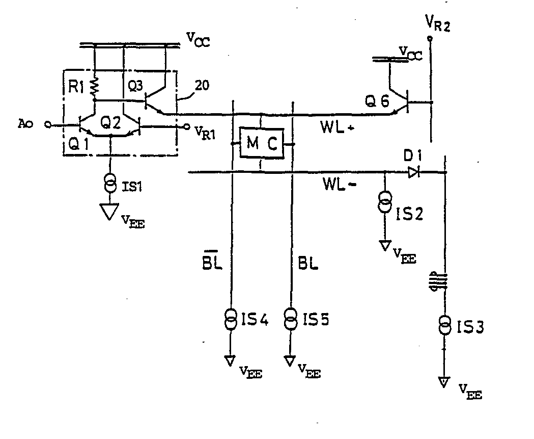
(57) @ A bipolar static memory device comprising clamping circuits (Q6) to sustain the
potential on the word lines (WL+) in non-selected state at a specified level is disclosed. Each of the high potential
side word lines (WL+) is connected to a clamping circuit (Q6) formed from a pnpn transistor whose base
is supplied with a reference voltage (VR2) and whose emitter and collector are respectively connected to the word line (WL+) and a high potential source (Vcc). Each of the word lines is clamped at a common level slightly higher than the level
determined by the output voltage of each associated word driver gate (20) in non-selected
state, hence, the potential on the word lines in non-selected state can be uniform
throughout the memory device regardless of the nonuniformity of the values of the
resistors (R1) in the word driver gates (20).
|
|
