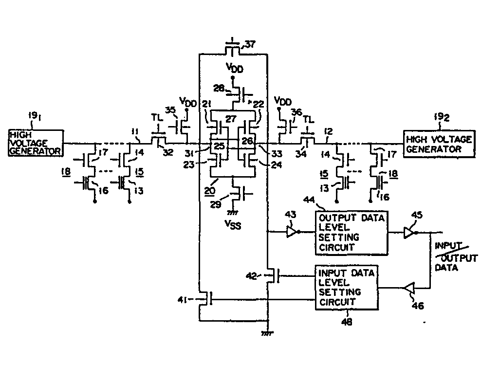
(57) A semiconductor memory device provided with first and second bit lines (11, 12),
each of which is connected to a memory cell (15) comprising a nonvolatile transistor
(13) and a dummy cell (18) comprising a nonvolatile transistor (16). The first and
second bit lines (11, 12) are respectively connected to high voltage generators (19"
19,) which are applied at the time of data programming. At the time of data reading,
data-detecting and storing means (20) comprising a flip-flop circuit (27) detects
data, while amplifying a potential difference between the first and second bit lines.
At the time of data writing, the data detecting and storing means (20) temporarily
stores data in accordance with the contents of externally supplied writing data. A
first switching transistor (32) is provided between the first data input-output node
of the data-detecting and storing means and the first bit line. The second switching
transistor (34) is connected between the second data input-output node of the data-detecting
and storing means and second bit line. The paired switching transistors are controlled
in accordance with the operation mode of the memory device.
|
|
