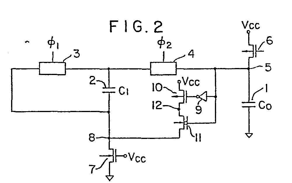
(57) A timer circuit which is used for write and erase time control of a semiconductor
memory, and configured so as to transfer a charge of a charge storage capacitor (1)
to a charge pump capacitor (2) through a first transfer gate (4) thereafter to repeatedly
effect a discharge operation by using a second transfer gate (3) thereby to gradually
reduce a charge of the charge storage capacitor (1), thus performing a timer operation,
characterized in that there is provided a circuit (7, 9, 10, 11, 12) for making an
adjustment such that a voltage applied to the charge pump capacitor (2) is smaller
than a voltage applied to the charge storage capacitor (1).
|
|
