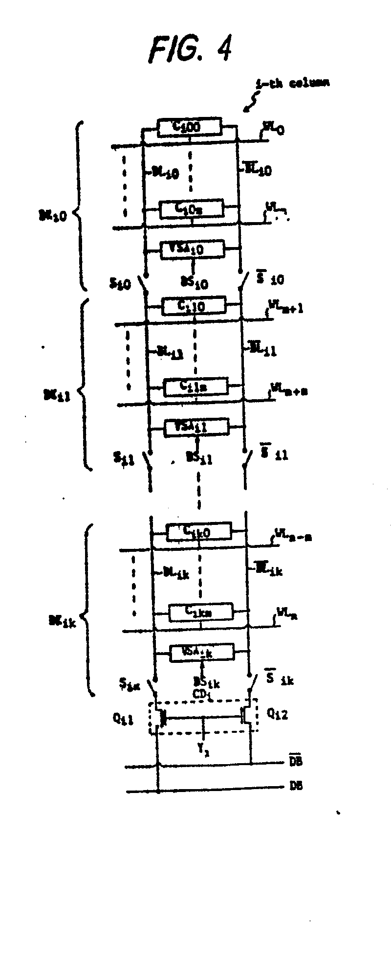
(57) The memory device has each pair of bit lines divided into blocks (BKi0,---, BKik) each comprising memory cells (Ci00, ---, C10m; ---; Ciko, ---, Cikm), switching elements (Sio, Sio; ---) Sik, Sik) inserted into the bit lines, and a block sense amplifier (VSAi0, ---, VSAik). Means responsive to the selection of a memory cell are provided to activate only
the sense amplifier of the block containing the selected memory cell, and the switching
elements are controlled to make ON only the ones of the selected block and of each
block located between the selected block and the data bus. The sense amplifiers (VSAio, ---, VSAik) have different driving abilities, such that the driving ability increases
as the distance between the corresponding blocks and the data bus increases. The differences
in driving ability can be obtained by using MOS transistors of different channel sizes
in the different blcok sense amplifiers.
|
|
