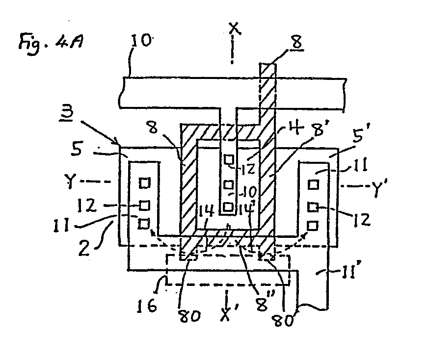
(57) A MIS FET is provided with an additional gate electrode (8") (referred to as a suppression
gate electrode) which extends along a boundary region between a MIS FET active region
(3) and a field oxide film (2) under a drain wiring (11'). When the drain wiring is
impressed to a voltage high enough to induce in the substrate (1) an inversion layer
(6") of the same polarity as the MIS FET channel, a parasitic transistor Tr, is formed
in parallel with the MIS FET and increases the leakage current. The supression gate
electrode of the present invention forms an interrupting transistor Tr2 connected in series with the parasitic transistor and cuts off the leakage current.
|
|
