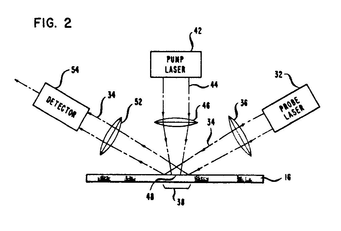
(57) Individual defects in or near the surface of a silicon wafer (16) are detected by
directing a time-modulated laser beam (44), having an energy level above the bandgap
energy of the silicon material, towards the wafer. The beam (44) is focused to a one
to two micron spot (48) on the wafer surface to photoexcite (i.e., pump) a high density
of electrons and holes which changes the infrared reflectance in the area of the pumped
spot. A probe beam (34) of infrared radiation is directed at the surface (0.126 square
mm in area) of the substrate (16) and at a small angle thereto and the reflection
thereof monitored by a detector (54). The pumped spot (48) is raster scanned within
the area of the probe beam spot (38). The detector (54) detects only that portion
of the intensity of reflected probe beam (34) that is modulated by the pump beam frequency
to create a video display having a high spatial resolution showing individual defects.
(FIG. 2).
|
|
