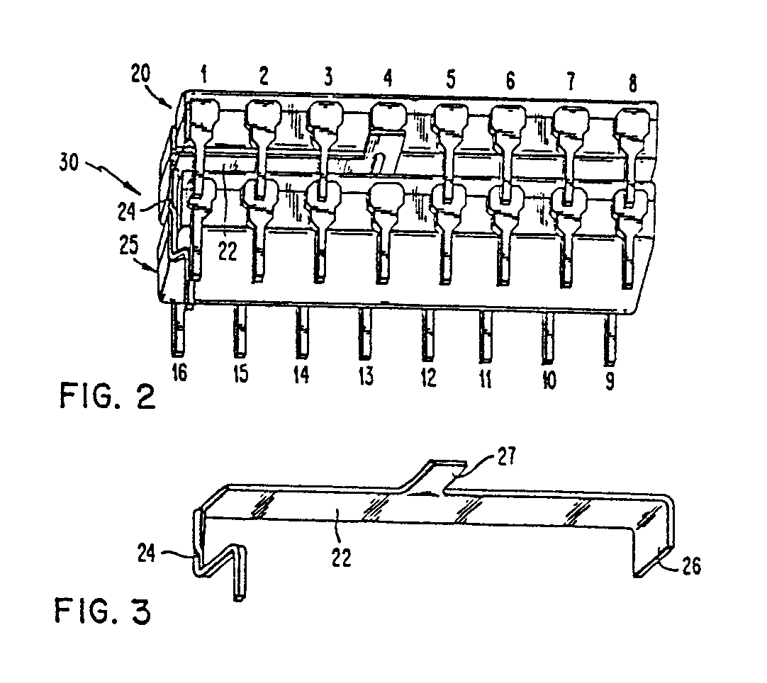
(57) A module (30) formed of stacked integrated circuit chips (20, 25) having similar
functional pin assignments includes a connector strap (22) which contacts the select
or enable pin (4) of the upper chip and forms an extra pin (24) so that each chip
in the module can be separately selected. The remaining overlapping pins of the stacked
chips are connected in parallel to form a module occupying the same area on a printed
circuit board or other second level package as that of one of the individual chips.
According to one embodiment of the invention two industry standard memory chips are
stacked to form a double density memory module. The connector strap (22) extends from
the chip enable pin (4) of the upper chip (20), between the chips, and down one side
of the lower chip to form a pin (24). According to another aspect of the invention
the connector strap extends the length of the upper surface of the lower chip. One
end (26) of the strap (22) is bent over one end of the lower chip, the other end (24)
of the strap being bent over the other end of the chip and extending downward to form
the upper chip select pin. A portion (27) of the connector strap near the chip select
pin (4) of the upper chip is bent upwards to form a connection thereto. The strap
is thus urged against the lower chip and held in place while the module is assembled.
|
|
