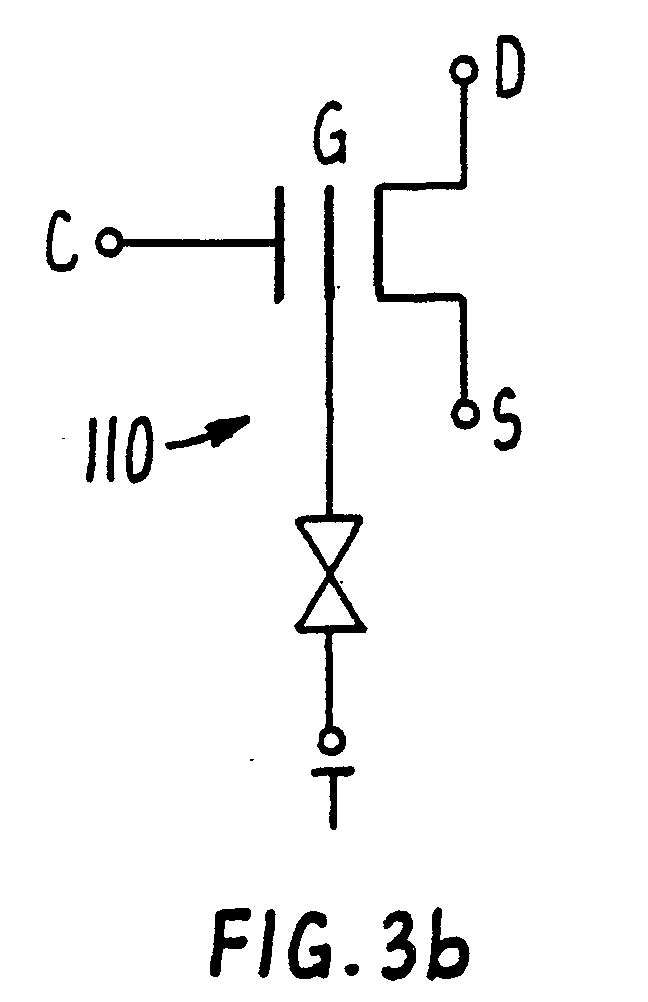
(57) In this invention, an Electrically Alterable Non-Volatile Memory (EANOM) cell is
disclosed. The EANOM cell comprises an MOS transistor, having a source, a gate and
a drain. The EANOM cell also has a two-terminal tunnel device, one end of which is
connected to the gate of the MOS transistor. The other terminal being labelled "T".
The tunnel device causes charges to be stored or removed from the gate of the MOS
transistor. In a preferred embodiment, a four-terminal EANOM cell is disclosed. The
four terminals of the EANOM cell are terminals T, S (source of the MOS transistor),
D (drain of the MOS transistor) and a terminal C which is capacitively coupled to
the gate of the MOS transistor. The EANOM cell can be used in a memory circuit to
increase the reliability thereof. Two or more EANOM cells are connected in tandem
and operate simultaneously. Catastrophic failure of one EANOM cell results in an open
circuit with the other EANOM cell continuing to function.
|
|
