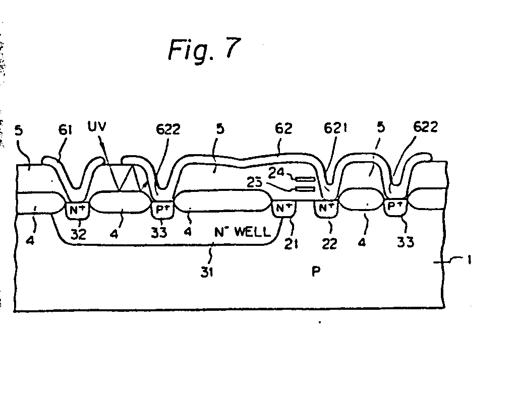
(57) A semiconductor memory device including a substrate (1) having one conductivity type;
read only memory element formed in the substrate for storing fixed information, the
element having a control gate (24), a floating gate (23), a source region (22), and
a drain region (21), both of the regions having an opposite conductivity type to that
of the substrate; a first region (33) having the above one conductivity type which
surrounds the element; a light shield layer (62), connected to the source region and
the first region, for covering the element; a second region (32) having the opposite
conductivity type which is located outside of the first region for taking out the
drain region; and a well region (31) having the opposite conductivity type, the well
region linking the drain region (21) and the second region (32), a part of the first
region (33) being formed in the well.
|
|
