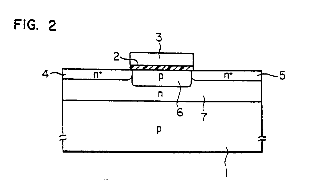
(57) The present invention relates to a semiconductor device comprising a semiconductor
substrate (l) of a first conductivity type or an insulator, a source (4) comprising
an impurity layer of a second conductivity type disposed on said semiconductor substrate
or said insulator, a drain (5) comprising an impurity layer of the second conductivity
type disposed on said semiconductor substrate or said insulator, an impurity layer
(6) of the first conductivity type formed between said source and said drain, a gate
(3) formed on said impurity layer of the first conductivity type via an insulation
film, and an impurity layer (7) of the second conductivity type having an impurity
concentration lower than that of said source and said drain, said impurity layer of
the second conductivity type being disposed between said source, said drain and said
impurity layer of the first conductivity type, and said semiconductor substrate of
the first conductivity type or said insulator.
|
|
