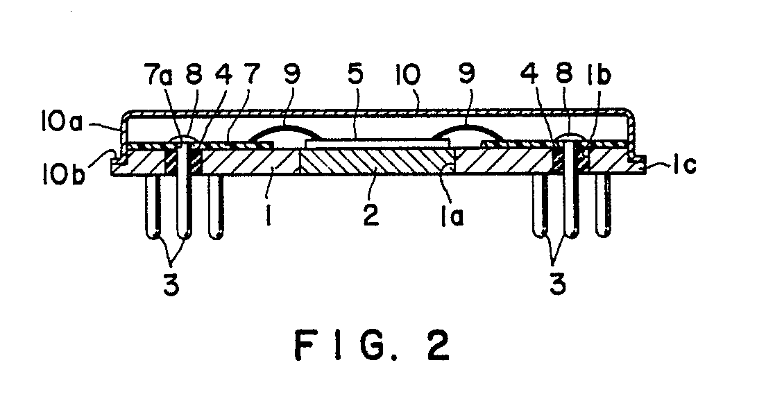
(57) A semiconductor chip (5) is mounted and fixed onto a stem (1). A wiring substrate
(7) is mounted and fixed around said semiconductor chip (5) on said stem (1). A number
of through-holes (1b, 7a) are provided so as to penetrate the stem and the wiring
substrate, and a number of lead-pins (3) are inserted into said respective through-holes
to extrude from the lower surface of said stem (1). Said semiconductor chip and said
wiring substrate are covered by and hermetically sealed to metallic shell (10). The
input-output terminals of the electric circuits formed on the semiconductor chip(5)
are connected respectively to said lead-pins (3) through wiring layer formed on said
wiring substrate (7). In such construction, it is possible to obtain a positive hermetic
sealing which is adaptable to multi-pin construction, thereby to reduce the manufacturing
cost of semiconductor packages.
|
|
