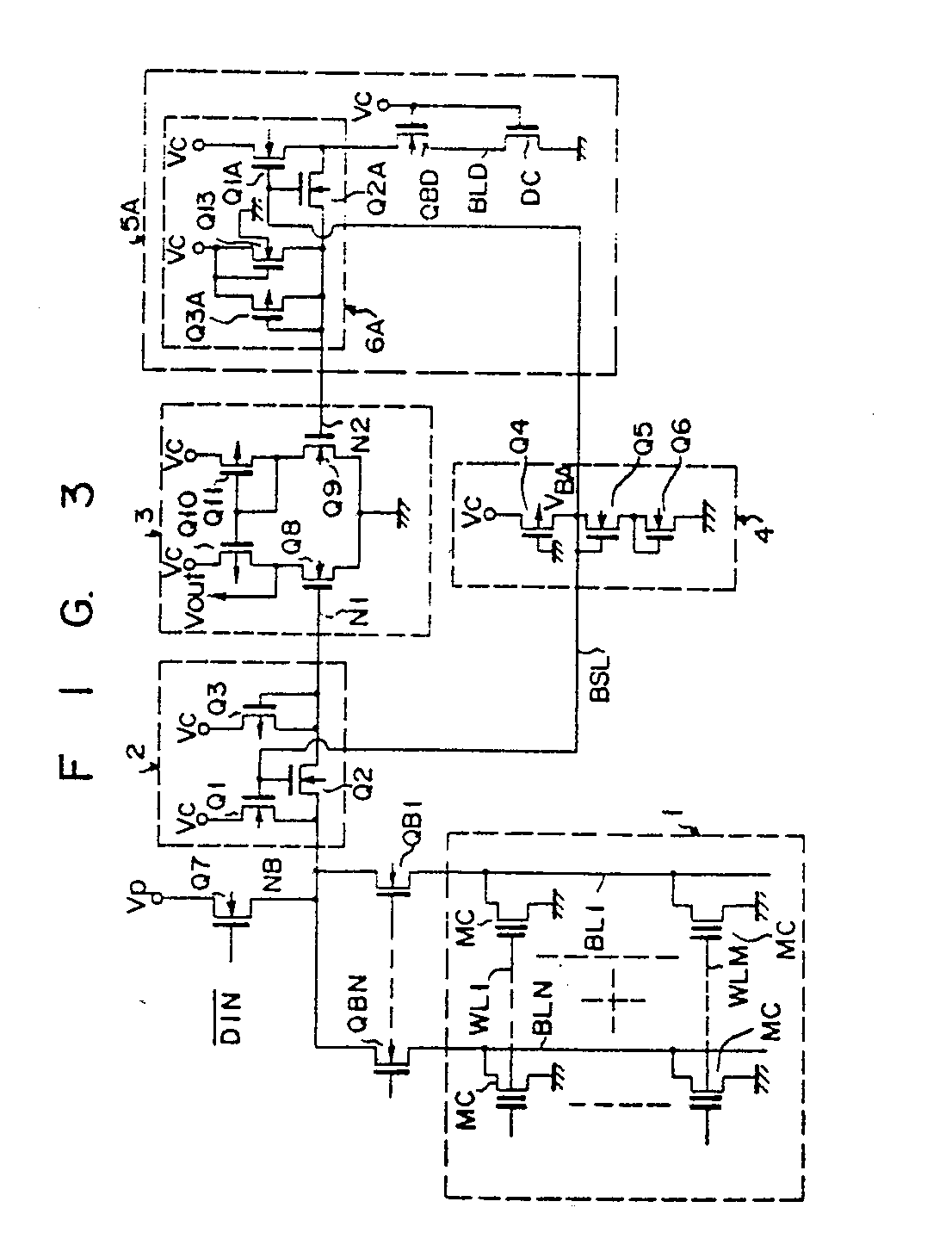
(57) A sense amplifier circuit comprises a first amplifier circuit (Q₁, Q₂) for detecting
the data from a memory cell and generating an output signal in accordance with the
detected data, a first load MOS transistor (Q₃) of one conductivity type connected
between an output terminal of the first amplifier circuit (Q₁, Q₂) and a power source
terminal (VC), a second amplifier circuit (Q1A, Q2A) for detecting the data from a dummy cell and generating an output signal in accordance
with the detected data, a second load MOS transistor (Q3A) of one conductivity type and a third load MOS transistor (Q₁₃) which are connected
in parallel between an output terminal of the second amplifier circuit (Q1A, Q2A) and the power source terminal, and a comparator (3) for comparing the output signals
from the first and second amplifier circuits (Q₁, Q₂, Q1A, Q2A) and generating an output signal in accordance with the result of the comparison.
The third load MOS transistor (Q₁₃) is a MOS transistor of an opposite conductivity
type whose back gate is connected to a reference potential terminal.
|
|
