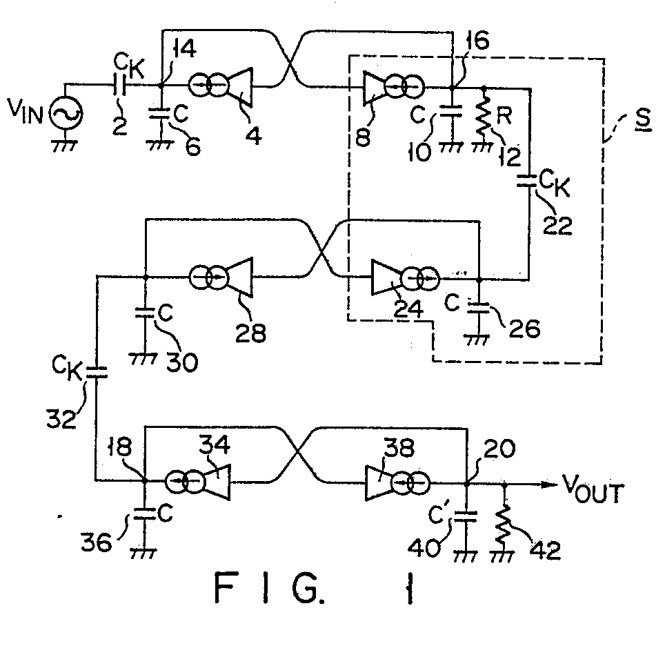
(57) A loop circuit of a band-pass filter is constituted by connecting two integrating
circuits (4, 6; 8,10 or 34, 36; 38, 40) each including a current source (4; 6 or 34;
38) and a capacitor (6; 10 or 36; 40) connected to an output terminal of thereof,
so that an input terminal of one (4, 6; 34, 36) of the integrating circuits is connected
to an output terminal of the other (8, 10; 38, 40) and an output terminal of one of
the integrating circuits is connected to an input terminal of the other. At least
two sets of the loop circuits (4 -10; 34 - 40) are used, and these loop circuits are
coupled by a capacitor (32). Two termination resistors (12; 42) are connected to an
output terminal of a start loop circuit and an output terminal of an end loop circuit,
respectively. A coupling capacitor (2) is connected to an input terminal of the start
loop circuit (4 - 10), and an input signal is input to the start loop circuit (4 -
10) through the coupling capacitor (2). An output signal is output from an output
terminal of the end loop circuit (34-40).
|
|
