(19)
(11) EP 0 288 035 A3

(12) EUROPEAN PATENT APPLICATION

(88) Date of publication A3:
07.02.1990 Bulletin 1990/06

(43) Date of publication A2:
26.10.1988 Bulletin 1988/43

(21) Application number: 88106322.6

(22) Date of filing: 20.04.1988
(51) International Patent Classification (IPC)4H03C 1/60, H03C 7/02, G01S 13/02
(84) Designated Contracting States:
DE FR GB SE

(30) Priority: 20.04.1987 JP 98367/87

(71) Applicant: SHARP KABUSHIKI KAISHA
Osaka 545 (JP)

(72) Inventors:
  • Higashi, Kazutada
    Tenri-shi Nara-ken (JP)
  • Tokuda, Masamori
    Ayama-gun Mie-ken (JP)
  • Nakano, Hiroshi
    Tenri-shi Nara-ken (JP)
  • Ohta, Tomozo
    Ikoma-shi Nara-ken (JP)

(74) Representative: TER MEER - MÜLLER - STEINMEISTER & PARTNER 
Mauerkircherstrasse 45
81679 München
81679 München (DE)


(56) References cited: : 


    (54) SSB modulator


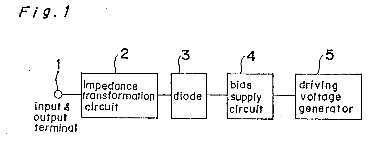
    (57) The SSB modulator according to the present invention is comprised of a driving voltage generator (5), a diode (3), a bias supply circuit (4), an impedance transformation circuit (2) and an input/output terminal (1). It is so arranged in the SSB modulator that the impedance of the diode (3) is changed by changing the driving voltage impressed to the diode (3), resulting in the mismatching of the impedance, which leads to generation of the reflected wave. Therefore, by changing the amplitude and the phase of the above-obtained reflected wave, SSB modulation is effected. Accordingly, the SSB modulator of the present invention requiring no particular side band filter is compact in size, light and weight and low in manufacturing cost, with a simple structure of the circuit.


    Search report