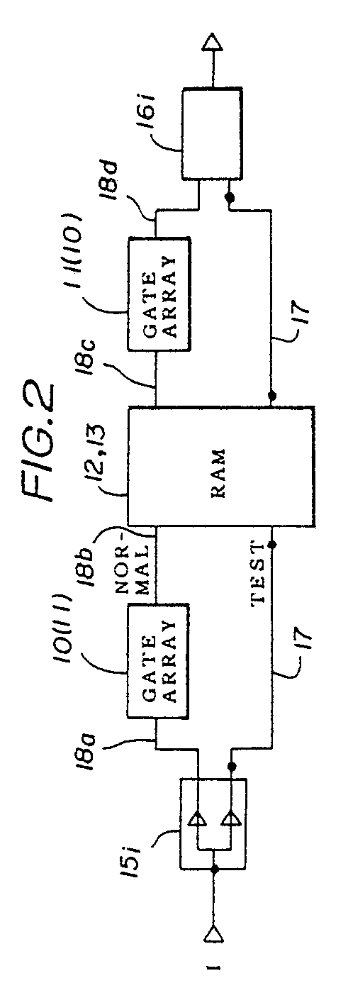
(57) A semiconductor integrated circuit device has a normal mode and a test mode for testing
a memory thereof, and comprises input/output buffer parts (15, 16) having input/output
terminals, at least one gate array (10, 11), at least one memory (12, 13), a first
interconnection (18a-18d) for coupling the input/output buffer parts, the gate array
and the memory and routed depending on a logic operation to be carried out by the
semiconductor integrated circuit, and a second interconnection (17) for coupling
the input/output buffer parts, the gate array and the memory, where the second interconnection
is fixed regardless of the logic operation to be carried out by the semiconductor
integrated circuit. The input/output buffer parts comprise a first input/output part
(15₁, ...) having a first terminal (15P) which is used in common as an input terminal
of the first interconnection for receiving a normal input signal in the normal mode
and an input terminal of the second interconnection for receiving a test signal in
the test mode, and a second input/output part (16₁, ...) having a second terminal
(22) which is used in common as an output terminal of the first interconnection and
an output terminal of the second interconnection.
|
|
