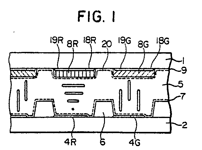
(57) Disclosed is a color liquid crystal display device having a plurality of pixels (4R,
4G, 4B), in which conductive films (19R, 19G, 19B) are arranged at regions corresponding
to the respective pixels, a light-shielding conductive layer (18R, 18G, 18B) is connected
to the conductive films and extends in a region between the pixels, and color filters
(8R, 8G, 8B) are formed on the conductive films. In the method of manufacturing such
color liquid crystal display device, a light-shielding conductive layer is formed
on a substrate (2), part of the light-shielding layer corresponding to a pixel for
which a filter is to be formed is removed from the substrate on which the light-shielding
layer is formed and simultaneously the light-shielding layer is partially removed
so that portions thereof corresponding to at least pixels having different colors
are electrically insulated from each other, a conductive film is formed at a portion
corresponding to the pixel for which the filter is to be formed, and films having
colors corresponding to those of the respective pixels are formed on the surface of
the conductive film.
|
|
