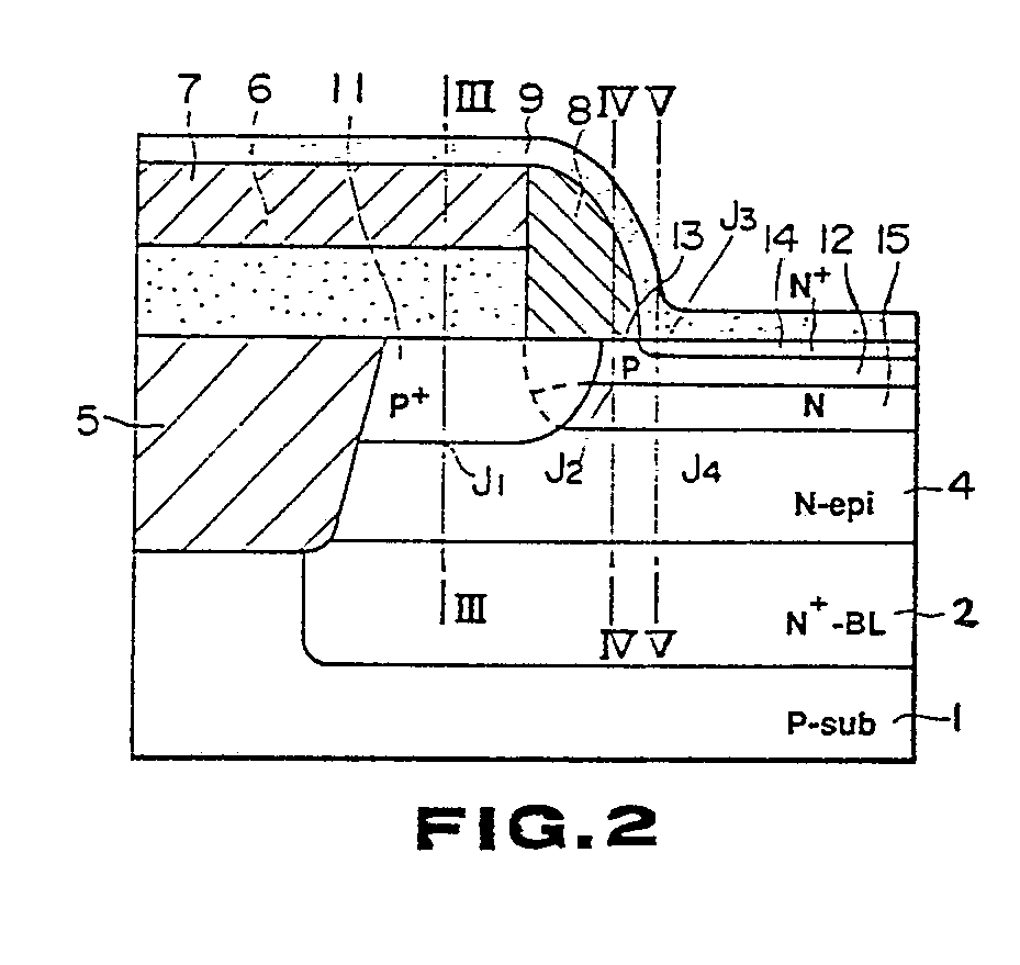
(57) A vertical type bipolar transistor has a base region on a semiconductor substrate
(1, 2, 4) formed by a graft base region (11), an intrinsic base region (12) separated
from the graft base region (11) and having an emitter region (14) within it, and a
link impurity diffusion region (13) linking the graft and intrinsic base regions (11,
12). During production, the graft base region (11) is formed by diffusion of impurities
from a base contact electrode layer (6) and the emitter region (14) formed in the
intrinsic base region (12) may be formed in self-alignment. In the vicinity of the
junction between the base region and the semiconductor substrate (1, 2, 4), there
is formed a diffusion suppression region (15) composed of an impurity diffusion region
of a conductivity type opposite to that of the base region; this prevents the depth
of the junction from being increased.
|
|
