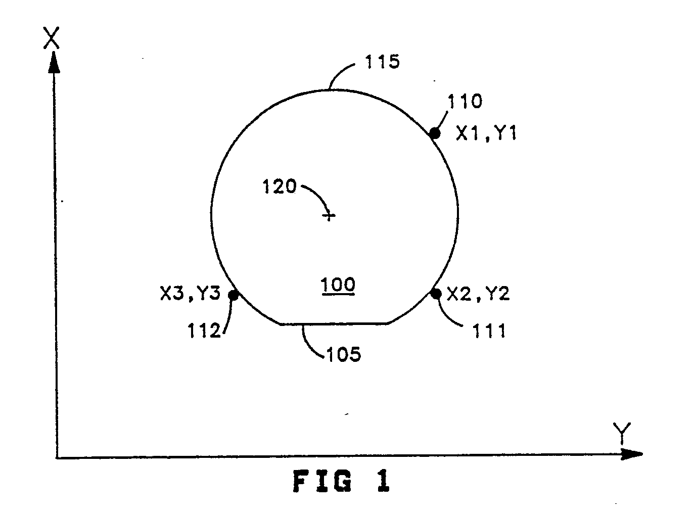
(57) A new and improved method and apparatus for profiling wafers (100), and for uniquely
identifying the dies formed thereon, wherein the method includes the step of locating
a set of reference points (110, 111) along the periphery of the wafer, relative to
a predetermined coordinate system. Next, the equation of a hypothetical circle which
substantially contours the periphery of the wafer, and which passes through the reference
points, is defined. The coordinates (a,b) of the center (120) of the hypothetical
circle, as well as the coordinates of an arbitrary reference die (102) on the wafer,
are then derived from the equation of the hypothetical circle. Subsequently, the entire
surface of the wafer is mapped relative to the center or to the reference die, by
utilizing predetermined stepping dimensions.
|
|
