(19)
(11) EP 0 343 720 A3

(12) EUROPEAN PATENT APPLICATION

(88) Date of publication A3:
28.02.1990 Bulletin 1990/09

(43) Date of publication A2:
29.11.1989 Bulletin 1989/48

(21) Application number: 89201245.1

(22) Date of filing: 17.05.1989
(51) International Patent Classification (IPC)4H01L 21/304, H01L 21/78
(84) Designated Contracting States:
DE FR GB IT NL

(30) Priority: 23.05.1988 US 197544

(71) Applicant: Philips Electronics N.V.
5621 BA Eindhoven (NL)

(72) Inventor:
  • Vokoun, Edward Richard
    NL-5656 AA Eindhoven (NL)

(74) Representative: Rensen, Jan Geert et al
INTERNATIONAAL OCTROOIBUREAU B.V., Prof. Holstlaan 6
5656 AA Eindhoven
5656 AA Eindhoven (NL)


(56) References cited: : 
   
     
    Remarks:
    The title of the invention has been amended (Guidelines for Examination in the EPO, A-III, 7.3).


    (54) Semiconductor wafer and method of dividing it


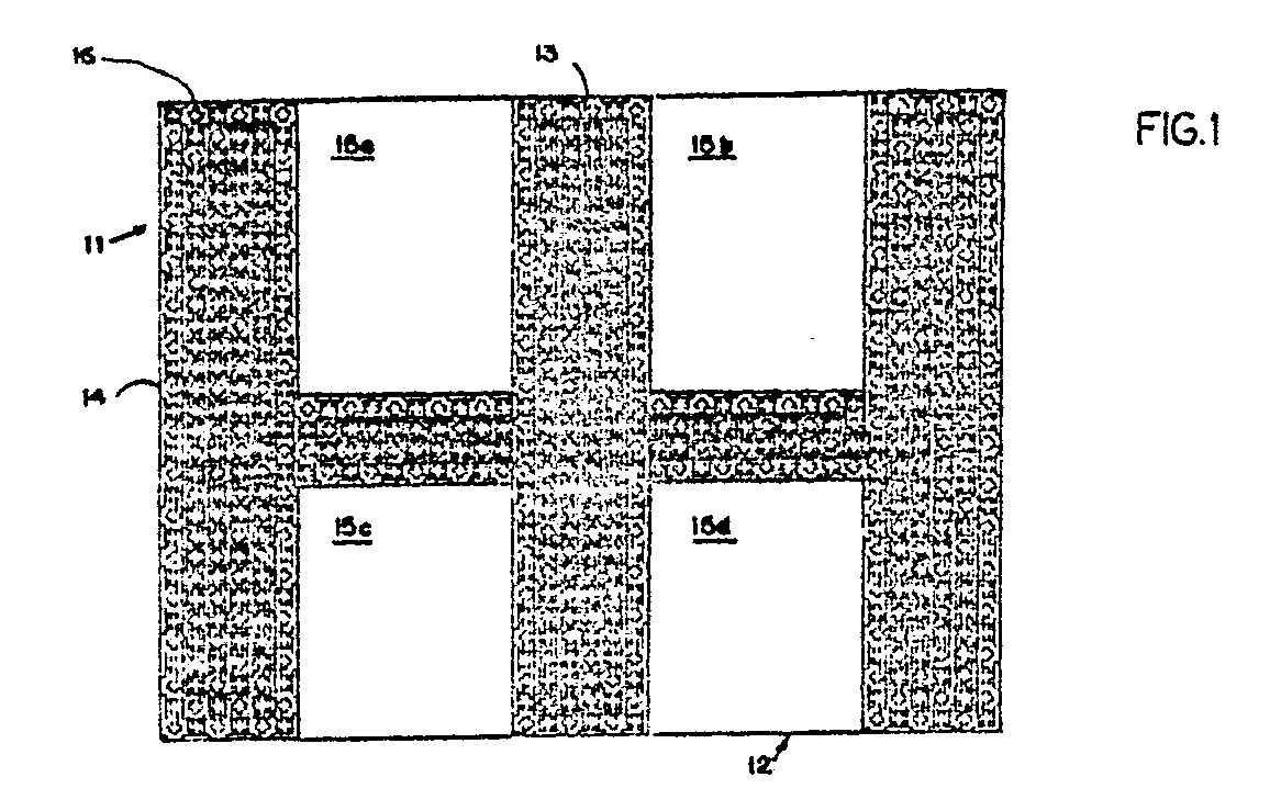
    (57) A semiconductor wafer (11) which comprises at least two semiconductor devices (15a, 15b,...), each surrounded by a scribe lane (14) which at least partially is covered by a metal film (13). In said metal film (13) a plurality of perforations (16) such as hloes, slots, slits, rectangles, squares, crosses etc are formed. According to the invention the distance between said perforations (16), in any direction, is not greater than about 7 to 10 microns. Thus, after separation of the semiconductor devices (15a, 15b), for example by sawing along the device lane, no metal shards larger than 10 microns will be present on the separated devices.


    Search report