|
(11) | EP 0 356 099 A2 |

| (12) | EUROPEAN PATENT APPLICATION |
|
|
|
|
|||||||||||||||||||||||||||
| (54) | Electrochromic device |
| (57) The present invention relates to an electrochromic device which comprises a first
electrode layer, an intermediate layer including an electrochromic layer, a second
electrode layer; said first electrode layer, said intermediate layer and said second
electrode layer being laminated in succession, and an electrode member connected to
one of said first and second electrode layers and extending in a predetermined direction
perpendicular to the direction of lamination of said first electrode layer, said intermediate
layer and said second electrode layer. The resistance R₁, R₂ respectively of said first and second electrode layers and the internal resistance R₃ of said intermediate layer satisfy the predetermined condition. |
BACKGROUND OF THE INVENTION
Field of the Invention
Related Background Art
[0002] A phenomenon of reversible coloration by reversible electrolytic oxidation or reduction under voltage application is called electrochromism.
[0003] Various attempts have been made, since more than 20 years ago, to prepare electrochromic devices (ECD) utilizing an electrochromic material showing such electrochromic phenomenon and capable of coloration and color erasure by voltage application, and to utilize such ECD for a light control device such as an anti-glare mirror, or a 7-segment numeric display unit.
[0004] For example, the U.S. Patent No. 3,829,196 discloses a totally solid-state ECD composed of a transparent electrode film (cathode), a tungsten trioxide film, an insulating film for example of silicon dioxide, and an electrode film (anode) laminated in succession on a glass substrate.
[0005] The tungsten trioxide (WO₃) film is colored blue when a voltage is applied to said ECD, and returns to the colorless state when an inverse voltage is applied. The mechanism of the coloration and color erasure is not fully clarified, but it is estimated that the coloration and color erasure of WO₃ is governed by a small amount of water present in the WO₃ film and the insulating film (ion conductive layer).
[0006] The reaction formulae are estimated as follows:
H₂O → H⁺ + OH⁻
(WO₃ film: cathode) WO₃ + nH⁺ + ne⁻ → HnWO₃
colorless, transparent colored
(insulating film: anode) OH⁻ → ½H₂O + ¼O₂↑+ ½e⁻
[0007] Also there is already known an ECD composed of an electrochromic layer capable of coloration by reduction (for example WO₃), an ion conductive layer, and a layer capable of reversible electrolytic oxidation (for example iridium oxide or iridium hydroxide) laminated in succession between an upper electrode and a lower electrode for applying a pre-determined voltage.
[0008] At least one of the electrode layers directly or indirectly sandwiching the electrochromic layer has to be transparent in order to show the coloration and color erasure to the exterior, and both electrode layers have to be transparent in case of a transmissive ECD.
[0009] It is already known that a transparent electrode can be prepared for example from SnO₂, In₂O₃ ITO (SnO₂ - In₂O₃ mixture) or ZnO, but these materials are of relatively low transparency and have to be made thin. Because of this fact, and also because of other reasons, the ECD is usually formed on a substrate such as a glass plate or a plastic plate.
[0010] Also for certain applications, a sealing substrate, for protecting the device, is positioned opposite to the substrate of the device, and the device is sealed for example with epoxy resin.
[0011] However, the conventional ECD'S have been associated with a drawback that the coloration is very slow and is not uniform, and said uneven coloration has been particularly marked in a large-sized ECD.
SUMMARY OF THE INVENTION
[0012] The object of the present invention is to provide an ECD capable of showing uniform coloration even in a large size.
[0013] The above-mentioned object can be attained, according to the present invention, by a certain relationship of the resistances of the intermediate layer including the electrochromic layer, and the upper and lower electrodes sandwiching said intermediate layer.
BRIEF DESCRIPTION OF THE DRAWINGS
[0014]
Fig. 1 is a schematic view showing the current flow in an ECD , for explaining the principle of the present invention;
Fig. 2 is a schematic view showing the current flow in an ECD embodying the present invention;
Fig. 3 is a schematic cross-sectional view of an ECD embodying the present invention; and
Fig. 4 is a plan view of an ECD for explaining the definition of conditions of the present invention.
DESCRIPTION OF THE PREFERRED EMBODIMENTS
[0016] At first explained is the relationship of the resistances of the intermediate layer, including the electrochromic layer, and the upper and lower electrodes sandwiching said intermediate layer, in a conventional ECD.
[0017] In the conventional ECD, the resistance R₁ of the upper electrode layer, the resistance R₂ of the lower electrode layer and the internal resistance R₃ of the intermediate layer sandwiched between said electrode layers satisfy following relation (1):
The resistance R₁ or R₂ of the upper or lower electrode is measured in a direction substantially perpendicular to the extending direction of a connection electrode provided in at least one of said upper and lower electrodes, and the resistance R₃ of the intermediate layer is measured in the direction of thickness thereof.
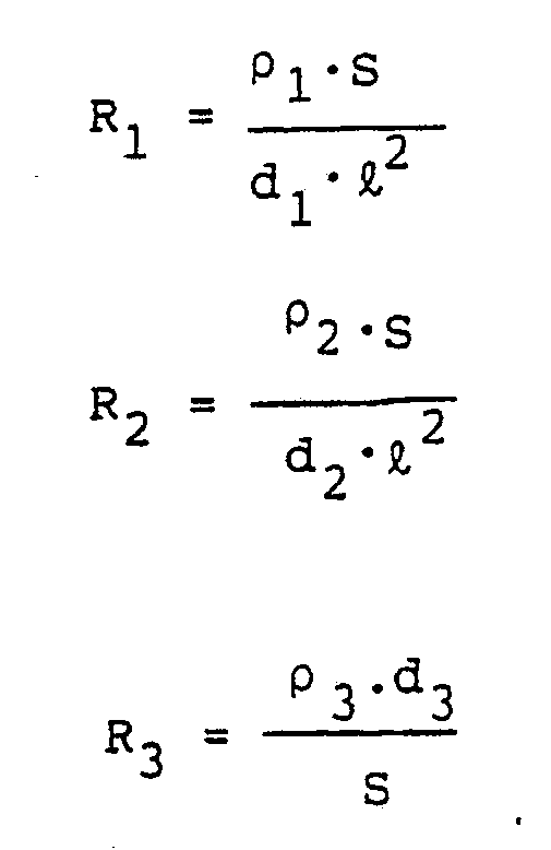
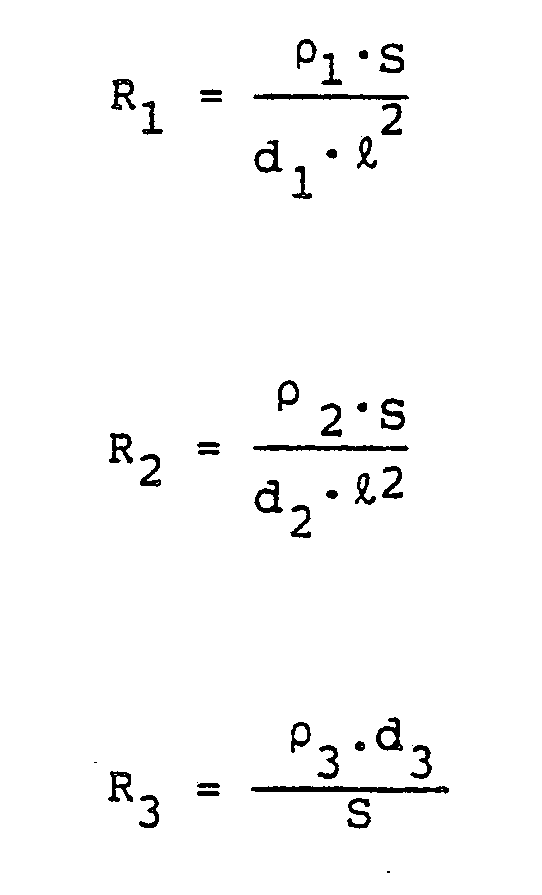
[0018] The resistances R₁, R₂ and R₃ are defined as follows:
wherein:
ρ₁: resistivity of upper electrode layer:
ρ₂: resistivity of lower electrode layer:
ρ₃: ion resistivity of intermediate layer;
d₁: thickness of upper electrode layer;
d₂: thickness of lower electrode layer;
d₃: thickness of intermediate layer;
ℓ: shortest length, in the extending direction of connection electrode, of the upper or lower electrode layer not connected to said connection electrode, the connection electrode and the intermediate layer; and
S : superposed area of the upper electrode layer, the intermediate layer and the lower electrode layer, when seen from the direction of lamination thereof.
[0019] It is also assumed that the resistance of the connection electrode is approximately zero, which means following conditions:
wherein
ρ₄ : resistivity of connection electrode; and
d₄: thickness of connection electrode.
[0020] Fig. 1 schematically shows the state of flow of current I when a voltage is applied to an ECD of the above-explained resistance relationship. Since the vertical resistance of the intermediate layer is smaller than the horizontal resistance of the upper electrode layer, most of the current I flows into the intermediate layer from an end of the upper electrode layer close to the connection electrode. Consequently, in a portion of the ECD close to the connection electrode, the aforementioned reaction proceeds to show faster and denser coloration, but in the central portion and in a portion opposite to said connection electrode, the coloration is much slower and paler due to much lower current density.
[0022] Also the erasure of coloration proceeds unevenly for the same reason, though the extent of unevenness is less marked than in the coloration.
[0023] According to the present invention, the aforementioned object is attained, in an electrochromic device composed of a laminate structure at least of an upper electrode, an electrochromic layer, and a lower electrode, by selecting the resistances R₁, R₂ of the upper and lower electrodes and the internal resistance R₃ of the electrochromic device so as to satisfy relations: R₁ < R₃ (5) and
R₂ < R₃ (6).
[0025] Fig. 2 shows the state of flow of the current I in the ECD of the present invention, when a voltage is applied across the upper electrode layer (positive side) and the lower electrode layer (negative side).
[0026] According to the present invention, since the resistances of two electrode layers and the internal resistance of the intermediate layer are so selected as to satisfy the above-mentioned relations:
R₁ < R₃ (5) and
R₂ < R₃ (6),
the current supplied from the connection electrode of the upper electrode layer (in the structure shown in Fig. 2), at first flows sufficiently in the upper electrode layer without voltage slope therein, and uniformly flows into the intermediate layer toward the lower electrode layer. Consequently the voltage across the upper and lower electrode layers is substantially constant in any part of the electrode layers in the horizontal direction.
[0027] For promoting the coloration and erasure of coloration the following condition:
is experimentally found preferable.
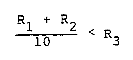
[0028] For achieving more uniform coloration, R₃ should be made as large as possible in comparison with R₁ and R₂, and experimentally preferred is a condition:
(R₁ + R₂) < R₃ (8),
or more particularly:
4(R₁ + R₂) < R₃ (9).
[0029] In the present invention, the relationship of magnitude of the resistances R₁, R₂ of the electrode layers is not important. If both layers are transparent electrodes, the resistance of the uppermost electrode layer tends to become larger, in practical film formation, than that of the electrode layer formed directly on the substrate.
[0030] The laminate structure of the ECD of the present invention is only required to have an upper electrode layer, an electrochromic layer and a lower electrode layer and there may be employed, for example, a structure employing a liquid electrochromic layer, an intermediate layer containing liquid electrolyte, a structure employing an organic electrochromic material or a structure utilizing metal ions such as lithium ions instead protons. However there is preferred a totally solid thin film structure composed of four layers such as electrode layer/electrochromic layer/ion conductive layer/electrode layer or five layers such as electrode layer/reduction coloring electrochromic layer/ion conductive layer/reversible electrolytic oxidation layer/electrode layer.
[0031] The transparent electrode can be formed, for example, of SnO₂, In₂O₃, or ITO. Such electrode layer can be generally formed by a vacuum thin film deposition technology such as vacuum evaporation, ion plating or sputtering.
[0033] The ion conductive layer can be composed, for example, of silicon oxide, tantalum oxide, titanium oxide, aluminum oxide, niobium oxide, zirconium oxide, hafnium oxide, lanthanum oxide or magnesium fluoride. The thin film of such materials is insulating to electrons depending on the method of film preparation, but is conductive to protons (H⁺) and hydroxyl ions (OH⁻).
[0034] The coloring and color erasing reactions of the electrochromic layer require cations, so that H⁺ ions or Li⁺ ions have to be incorporated in the electrochromic or other layer. The H⁺ ions need not necessarily be present from the beginning but can be generated under the voltage application, and water may be added instead of H⁺ ions. The amount of water can be very small, and the coloring and color erasing reactions may take place even by the moisture spontaneously entering from the air.
[0035] It is possible to place either of the electrochromic layer and the ion conductive layer above the other. Furthermore there may be provided a reversible electrolytic oxidation layer (eventually constituting an oxidation coloring electrochromic layer) or a catalytic layer in opposed relation to the electrochromic layer across the ion conductive layer.
[0036] Such layer may be composed, for example, of oxide or hydroxide of iridium, nickel, chromium, vanadium, rutenium or rhodium. Such materials may be dispersed in the ion conductive layer or in the transparent electrode, or may be used for dispensing the material of said layers. The opaque electrode layer may also serve as a reflective layer, and can be composed of a metal such as gold, silver, aluminum, chromium, tin, zinc, nickel, rutenium, rhodium or stainless steel.
[0037] The upper and lower electrode layers have to be connected to external wirings for charge (current) supply. However, in the use of a transparent electrode which is higher in resistance than the external wirings, a connection electrode of low resistance is superposed, in an area as large as possible, with (in contact with) the transparent electrode. Normally, the connection electrode of low resistance is formed as a belt in the peripheral area of the transparent electrode layer. Said electrode of low resistance can be composed of the materials for the above-mentioned opaque electrode layer, for example aluminum.
[0038] In the use of opaque electrode which is generally of low resistance, a part of said electrode can be used as the connection electrode.
[0039] Fig. 3 is a schematic cross-sectional view of an embodiment of the ECD of the present invention, wherein z-direction corresponds to the direction of thickness of the ECD.
[0040] At first on the entire surface of a rectangular or parallelogram glass substrate 10 (25 x 15 cm; area S = 375 cm²; length ℓ of connection electrodes for the upper and lower electrode layers = 25 cm) there was formed an ITO electrode layer of a thickness d₂ = 2 x 10⁻⁵ cm (resistivity ρ₂ = 2 x 10⁻⁴ Ω cm).
[0041] Then said ITO electrode layer was split into two portions, at an end part thereof by forming a narrow groove with etching or laser beam cutting, thereby forming a connection part 7 for the upper electrode, and a lower electrode layer 2.
[0042] Said connection part 7 and lower electrode layer 2 may be formed directly by masked evaporation of ITO.
[0043] On said lower electrode layer 2, there were formed, in succession, a reversible electrolytic oxidation layer 5 consisting of a mixture of iridium oxide and tin oxide, an ion conductive layer consisting of tantalum oxide, and a reduction coloring electrochromic layer 3 consisting of tungsten oxide.
[0044] The intermediate layer, consisting of the above-mentioned three layers 3, 4 and 5, has a thickness d₂ = 1.5 x 10⁻⁴ cm, and an ion resistivity ρ₃ = 2 x 10⁸ Ω·cm.
[0045] On the electrochromic layer 3, there was formed, by evaporation, an ITO electrode layer of a thickness d₁ = 2 x 10⁻⁵ cm (resistivity ρ₁ = 4 x 10⁻⁴ Ω·cm) as an upper electrode layer 1. Said ITO layer was formed so as to contact, at an end thereof, with the connection part 7 formed on the substrate 10.
[0046] The resistivity and ion resistivity of the layers can be varied by suitably selecting the conditions of film formation, such as Ar/O₂ ratio. degree of vacuum, film forming rate, substrate temperature, high-frequency power applied etc.
[0047] The resistances R₁, R₂ and R₃ of the layers are calculated as follows:
ρ₁/d₁ = 20 Ω
ρ₂/d₂ = 10 Ω
ρ₃·d₃ = 3 x 10⁴ Ωcm²
ℓ = 25 cm, S = 375 cm²
Consequently:
R₁ = ρ₁·S/d₁ℓ² = 12 Ω
R₂ =ρ₂·S/d₂ℓ² = 6 Ω
R₃ = ρ₃·d₃/S = 80 Ω
[0049] Then external wirings 11a, 11b were connected, by soldering or with conductive adhesive, to two phosphor bronze clips of square-C section of a length of 25 cm (connection electrodes) 8a, 8b, which were then mounted on end portions of the substrate 10 in such a manner that the clip 8a is in contact with the connection part 7 of the upper electrode while the clip 8b is in contact with a part of the lower electrode layer 2. In this case, the clips 8a, 8b constituting the connection electrodes are regarded as substantially zero resistance (constant potential in any part).
[0050] The shape and dimension of said clips 8a, 8b are so selected as to be capable of defining the position of a sealing substrate 6 to be explained later and masking the non-display portion in the peripheral part of the ECD.
[0051] Finally a sealing glass substrate 6, coated with epoxy sealing resin, was superposed on an area between the clips 8a, 8b and the sealing resin was hardened to complete the ECD of the present embodiment. A coloring voltage (+3 V) was applied, by a power source 12, across the upper and lower electrode layers 1, 2 of thus prepared ECD, whereby the ECD showed rapid and uniform coloration over the entire surface, reducing the transmittance of the light of 633 nm to 10 % after 20 seconds.
[0052] The transmittance remained in this state for a while even after the termination of voltage application, and was elevated to 70 % after application or an erasing voltage (-3 V) for 20 seconds.
[0053] For referecne, another ECD of same dimensions and thicknesses was prepared with modified resistivity ρ₁, ρ₂ and ion resistivity ρ₃ of the layers. Resistances were R₁ = 12 Ω , R₂ = 6 Ω , and R₃ = 0.15 Ω , so that:
[0054] In the same test as in the foregoing embodiment, this ECD showed uneven coloration and color erasure.
[0056] Fig. 4 is a plan view of a part of the ECD shown in Fig. 3, seen along Z-axis from above the upper electrode layer 1. For explaining the definition of S and ℓ , the structure shown in Fig. 4 is partly different from what is shown in Fig. 3.
[0057] S corresponds to the superposed area, when seen along z-axis, of the upper electrode 1, the intermediate layers 3, 4, 5 and the lower electrode 2. In the structure shown in Fig. 4, the area 21 of the lower electrode 2 is smallest among these. Consequently the area S corresponds to the area 21 of the lower electrode 2. On the other hand, if the area of the intermediate layers 3, 4, 5 is smallest among the upper electrode 1, said intermediate layers 3, 4, 5 and the lower electrode 2, the area S corresponds to the area of said intermediate layers. In Fig. 4, an area 22 indicates the remaining part of the lower electrode 2, excluding the area 21.
[0058] ℓ corresponds to the length ℓ₁ of the connection electrode 7 in the x-direction in Fig. 4, but it corresponds to the length ℓ₃ of the lower electrode 2 in the x-direction if it is shorter than said length ℓ₁. Also ℓ corresponds to the length ℓ₂ of the intermediate layers 3, 4, 5 if it shorter than the length ℓ₁ of the connection electrode 7 and the length ℓ₃ of the lower electrode 2.
[0059] In the structures shown in Figs. 3 and 4, the upper electrode 1 is provided with the connection electrode 7 but the lower electrode 2 is not provided with the connection electrode, because the lower electrode 2 is composed of a material same as that of the connection electrode 7 and is in itself suitable as the connection electrode. If the material of the lower electrode 2 is not suitable as the connection electrode 2, a connection electrode has to be connected also to the lower electrode 2. In such case ℓ₃ is the length, in x-direction of the connection electrode connected to the lower electrode 2.
1. An electrochromic device comprising:
a first electrode layer;
an intermediate layer including an electrochromic layer;
a second electrode layer; said first electrode layer, said intermediate layer and said second electrode layer being laminated in succession; and
an electrode member connected to one of said first and second electrode layers and extending in a predetermined direction perpendicular to the direction of lamination of said first electrode layer, said intermediate layer and said second electrode layer;
wherein the resistances R₁, R₂ respectively of said first and second electrode layers and the internal resistance R₃ of said intermediate layer satisfy following condition:
said resistances R₁, R₂ and R₃ being defined as follows:
wherein
ρ₁ : resistivity of upper electrode layer:
ρ₂ : resistivity of lower electrode layer:
ρ₃ : ion resistivity of intermediate layer:
d₁: thickness of upper electrode layer:
d₂: thickness of lower electrode layer;
d3: thickness of intermediate layer;
ℓ: shortest length, in the extending direction of connection electrode, among the upper or lower electrode layer not connected to said connection electrode, the connection electrode and the intermediate layer; and
S : superposed area of the upper electrode layer, the intermediate layer and the lower electrode layer, when seen from the direction of lamination thereof.
2. An electrochromic device according to claim 1, wherein the resistances R₁ and R₂
respectively of said first and second electrode layers and the internal resistance
R₃ of the second electrode layer satisfy following condition:
(R₁ + R₂) < R₃.
(R₁ + R₂) < R₃.
3. An electrochromic device according to claim 2, wherein the resistances R₁ and R₂
respectively of said first and second electrode layers and the internal resistance
R₃ of said intermediate layer satisfy following condition:
4(R₁ + R₂) < R₃.
4(R₁ + R₂) < R₃.
4. An electrochromic device according to claim 3, further comprising means for applying
a voltage between an electrode provided in said first electrode layer and an electrode
provided in said second electrode layer.
5. An electrochromic device comprising:
a first electrode layer;
an intermediate layer including an electrochromic layer;
a second electrode layer; said first electrode layer, said intermediate layer and said second electrode layer being laminated in succession; and
an electrode member connected to one of said first and second electrode layers and extending in a predetermined direction intersecting to the direction of lamination of said first electrode layer, said intermediate layer and said second electrode layer;
wherein the resistances R₁ and R₂ respectively of said first and second electrode layers and the internal resistance R₃ of said intermediate layers satisfy following conditions:
R₁ < R₃ and
R₂ < R₃
said resistances R₁, R₂ and R₃ being defined as follows:
wherein
ρ₁: resistivity of upper electrode layer;
ρ₂: resistivity of lower electrode layer:
ρ₃: ion resistivity of intermediate layer;
d₁: thickness of upper electrode layer;
d₂: thickness of lower electrode layer;
d₃: thickness of intermediate layer;
ℓ: shortest length, in said predetermined direction, among the first or second electrode layer not connected to the electrode member, the electrode member and the intermediate layer; and S: superposed area of the upper electrode layer, the intermediate layer and the lower electrode layer, when seen from the direction of lamination thereof.
6. An electrochromic device comprising an electrochromic layer disposed between first
and second electrode layers which are coupled, respectively, to first and second electrical
connection means, the resistivities of the layers being such that current flowing
between the first and second connection means is distributed substantially uniformly
over the area of the elctrochromic layer.