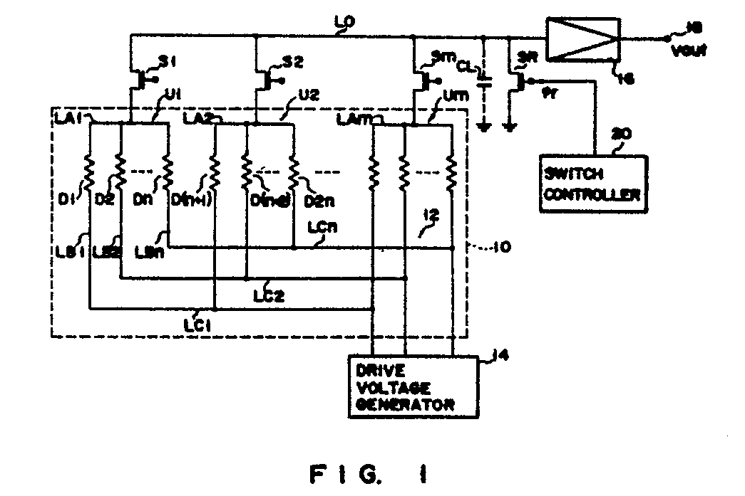
(57) A contact-type image sensor which has amorphous semiconductor photoconductive cells
(D1, D2, ..., Dnm) formed on a substrate and divided into cell units (U1, U2, ...,
Um) each consisting of a number of cells. A drive signal generator (14) is connected
to the cells (D1, D2, ..., Dnm) to sequentially select the cell units, thereby sequentially
activating the cells of any selected unit. A signal readout circuit (S1, S2, ...,
Sm, LO, CL, 16) is connected to the cell units, for generating a series of pixel signals
from pixel currents sequentially supplied from the cells of any selected unit. The
signal readout circuit includes a common signal output line (LO) connected to the
cell units, and a capacitor component (CL) connected to this output line, for sequentially
accumulating the pixel currents. The capacitor component (CL) is not a discrete element,
but is equivalent to the sum of the stray capacitance components inherently present
in the image sensor, such as parasitic capacitance components and the coupling capacitance
between the output line and the ground. An analog switch (SR) is connected between
the common signal output line (LO) and the ground. The analog switch (SR) operates
in response to a control pulse signal (φr) supplied from a switch controller (20),
thereby to reset the common signal output line every time one of the cells of each
unit cell is designated after a pixel current is read out from another cell adjacent
to this cell. Since the output line is thus reset, and the capacitor component (CL)
is thereby initialized, the attenuation ratio of each pixel current signal can be
reduced.
|
|
